1. Introduction
SRAM-based field-programmable gate arrays (FPGAs) need to protect the programming bitstream against reverse engineering and bitstream manipulation (tamper) attacks. Fielded systems are often the targets of attack by adversaries seeking to steal intellectual property (IP) through reverse engineering, or attempting to disrupt operational systems through the insertion of kill switches known as hardware Trojans. Internet-of-things (IoT) systems are particularly vulnerable, given the resource-constrained and unsupervised nature of the environments in which they operate.
FPGAs implementing a secure boot usually store an encrypted version of the programming bitstream in an off-chip non-volatile memory (NVM) as a countermeasure to these types of attacks. Modern FPGAs provide on-chip battery-backed random-access memory (RAM) or E-Fuses for the storage of a decryption key, which is used by vendor-embedded encryption hardware functions, e.g., the Advanced Encryption Standard (AES), within the FPGA in order to decrypt the bitstream as it is read from the external NVM during the boot process [
1]. Recent attack mechanisms have been shown to read out embedded keys, and therefore on-chip key storage threatens the security of the boot process [
2].
In this paper, we propose a physical unclonable function (PUF)-based key generation strategy that addresses the vulnerability of on-chip key storage. Moreover, the proposed secure boot technique is self-contained, in that none of the FPGA-embedded security primitives or FPGA clocking resources are utilized. We refer to the system as Bullet-Proof Boot for FPGAs (BulletProoF). BulletProoF uses a PUF implemented in the programmable logic (PL) side of an FPGA to generate the decryption key at boot time, and then uses the key for decrypting an off-chip NVM-stored second stage boot image. The second stage boot image contains PL components as well as software components, such as an operating system and applications. BulletProoF decrypts and programs the PL components directly into those portions of the PL side that are not occupied by BulletProoF using dynamic partial reconfiguration, while the software components are loaded into DRAM for access by the processor system (PS). The decryption key is destroyed once this process completes, minimizing the time the decryption key is available.
Similar to PUF-based authentication protocols, enrollment for BulletProoF is carried out in a secure environment. The enrollment key generated by BulletProoF is used to encrypt the second stage boot image. Both the encrypted image and the unencrypted BulletProoF bitstreams are stored in the NVM. During the in-field boot process, the first stage boot loader (FSBL) loads the unencrypted BulletProoF bitstream into the FPGA. BulletProoF reads the entire set of configuration data that has just been programmed into the FPGA using the internal configuration access port (ICAP) interface [
3], and uses this data as challenges to the PUF to regenerate the decryption key. Therefore, BulletProoF self-authenticates. The BulletProoF bitstream instantiates the SHA-3 algorithm, and uses this cryptographic function both to compute hashes and as the entropy source for the PUF. As we will show, BulletProoF is designed so that the generated decryption key is irreversibly tied to the data integrity of the entire unencrypted bitstream.
BulletProoF is stored unencrypted in an off-chip NVM, and is therefore vulnerable to manipulation by adversaries. However, the tamper-evident nature of BulletProoF prevents the system from booting the components present in the second stage boot image if tampering occurs, because an incorrect decryption key is generated. In such cases, the encrypted bitstring is not decrypted and remains secure.
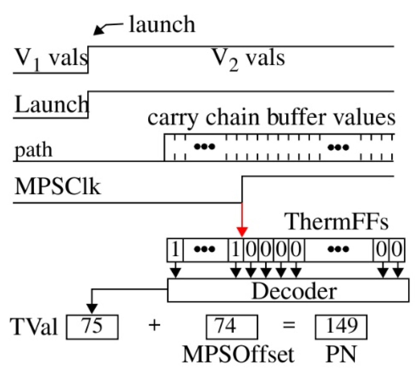
The hardware-embedded delay PUF (HELP) is leveraged in this paper as a component of the proposed tamper-evident, self-authenticating system implemented within BulletProoF. HELP measures path delays through a CAD-tool-synthesized functional unit—in particular, the combinational component of SHA-3 in the proposed system. Within-die variations that occur in path delays from one chip to another allow HELP to produce a device-specific key. Challenges for HELP are two-vector sequences that are applied to the inputs of the combinational logic that implements the SHA-3 algorithm. The timing engine within HELP measures the propagation delays of paths sensitized by the challenges at the outputs of the SHA-3 combinational block. The digitized timing values are used in the HELP bitstring processing algorithm, in order to generate the AES key.
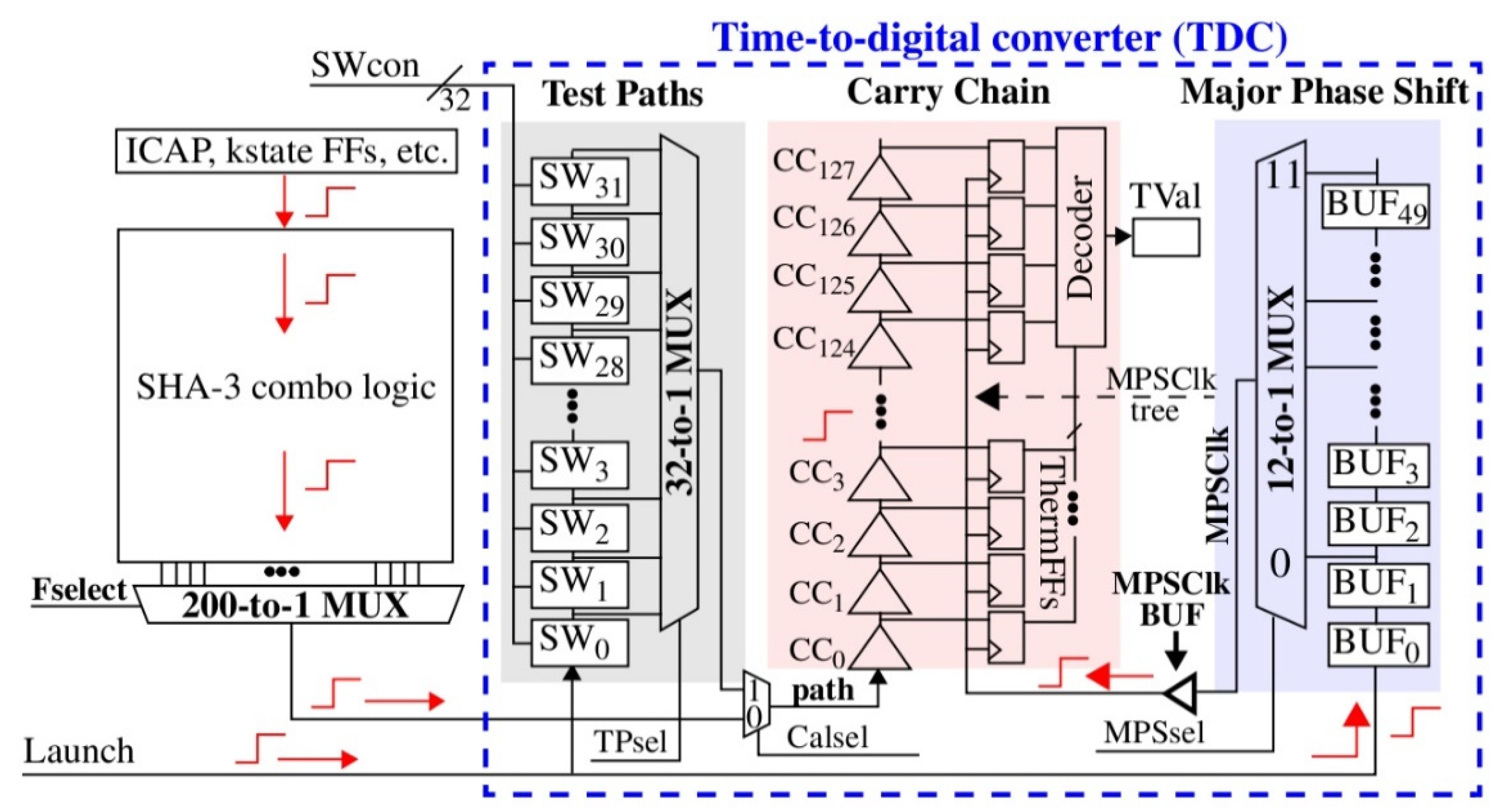
The timing engine times paths using either the fine-phase shift capabilities of the digital clock manager on the FPGA, or by using an on-chip time-to-digital-converter (TDC) implemented using the carry-chain logic within the FPGA. The experimental results presented in this paper are based on the TDC strategy.
The BulletProoF boot process is summarized as follows:
The first-stage boot loader (FSBL) programs the PL side with the unencrypted (and untrusted) BulletProoF bitstream.
BulletProoF reads the configuration information of the PL side (including configuration data that describes itself) through the ICAP, and computes a set of digests using SHA-3.
For each digest, the mode of the SHA-3 functional unit is switched to PUF mode, and the HELP engine is started.
Each digest is applied to the SHA-3 combinational logic as a challenge. Signals propagate through SHA-3 to its outputs, and are timed by the HELP timing engine. The timing values are stored in an on-chip block RAM (BRAM).
Once all timing values are collected, the HELP engine uses them (and helper data stored in the external NVM) to generate a device-specific decryption key.
The key is used to decrypt the second stage boot image components also stored in the external NVM and the system boots.
Self-authentication is ensured because any change to the configuration bitstream will change the digest. When the incorrect digest is applied as a challenge in PUF mode, the set of paths that are sensitized to the outputs of the SHA-3 combinational block will change (when compared to those sensitized during enrollment using the trusted BulletProoF bitstream). Therefore, any change made by an adversary to the BulletProoF configuration bitstring will result in missing or extra timing values in the set used to generate the decryption key.
The key generated by HELP is tied directly to the exact order and cardinality of the timing values. It follows that any change to the sequence of paths that are timed will change the decryption key. As we discuss below, multiple bits within the decryption key will change if any bit within the configuration bitstream is modified by an adversary, because of the avalanche effect of SHA-3 and because of a permutation process used within HELP to process the timing values into a key. Note that other components of the boot process, including the first-stage boot loader (FSBL), can also be included in the secure hash process, as well as FPGA-embedded security keys, as needed.
The rest of this paper is organized as follows. Related work is discussed in
Section 2. An overview of the existing Xilinx boot process is provided in
Section 3.
Section 4 describes the proposed BulletProoF system, while
Section 5 describes BulletProoF countermeasures, including an on-chip time-to-digital-converter (TDC), which leverages the carry-chain component within an FPGA for measuring path delays.
Section 6 presents a statistical analysis of bitstrings generated by the TDC as proof-of-concept. Conclusions are provided in
Section 7.
3. Overview of a Secure Boot under Xilinx
A hardwired 256-bit AES decryption engine is used by Xilinx to protect the confidentiality of externally stored bitstreams [
1]. Xilinx provides software tools to allow a bitstream to be encrypted using either a randomly generated or user-specified key. Once generated, the decryption key can be loaded through JTAG into a dedicated E-Fuse NVM or battery-backed BRAM (BBRAM). The power-up configuration process associated with fielded systems first determines whether the external bitstream includes an encrypted-bitstream indicator, and if so, decrypts the bitstream using cipher block chaining (CBC) mode of AES. To prevent fault injection attacks [
5], Xilinx authenticates configuration data as it is loaded. In particular, a 256-bit keyed hashed message authentication code (HMAC) of the bitstream is computed, using SHA-256 to detect tamper and to authenticate the sender of the bitstream.
During provisioning, Xilinx software is used to compute an HMAC of the unencrypted bitstream, which is then embedded in the bitstream itself and encrypted by AES. A second HMAC is computed in the field as the bitstream is decrypted, and compared with the HMAC embedded in the decrypted bitstream. If the comparison fails, the FPGA is deactivated. The security properties associated with the Xilinx boot process enable the detection of transmission failures, and attempt to program the FPGA with a non-authentic bitstream and tamper attacks on the authentic bitstream.
The secure boot model in modern Xilinx system-on-chip (SoC) architectures differs from that described above, because Xilinx SoCs integrate both programmable logic (PL) and processor components (PS). Moreover, the SoC is designed to be processor-centric, i.e., the boot process and overall operation of the SoC is controlled by the processor. Xilinx SoCs use public key cryptography to carry out authentication during the secure boot process. The public key is stored in an NVM and is used to authenticate configuration files, including the first-stage boot loader (FSBL), and therefore, the key provides secondary authentication and primary attestation.
The Xilinx Zynq 7020 SoC used in this paper incorporates both a processor (PS) side and programmable logic (PL) side. The processor side runs an operating system (OS), e.g., Linux, and applications on a dual core ARM cortex A-9 processor, which is tightly coupled with the PL side through an AMBA AXI interconnect.
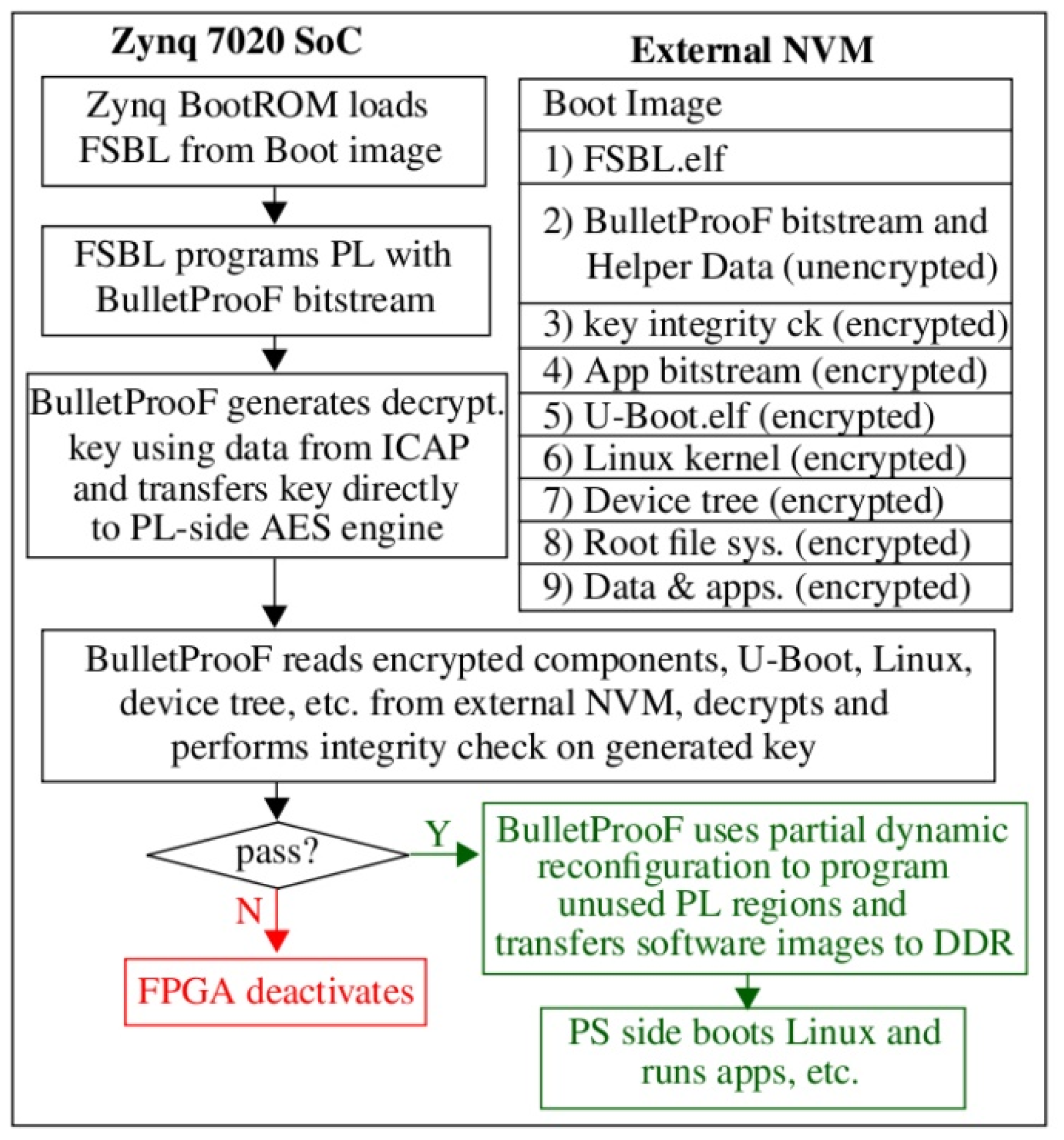
The flow diagram shown on the left side of
Figure 1 identifies the basic elements of the Xilinx Zynq SoC secure boot process. The Xilinx BootROM loads the FSBL from an external NVM to DRAM. The FSBL programs the PL side and then reads the second-stage boot loader (U-Boot), which is copied to DRAM, and passes control to U-Boot. U-Boot loads the software images, which can include a bare-metal application, or the Linux OS, as well as other embedded software applications and data files. A secure boot first establishes a root of trust, and then performs authentication on top of the trusted base at each of the subsequent stages of the boot process. As mentioned, Rivest–Shamir–Adleman (RSA) is used for authentication and attestation of the FSBL and other configuration files. The hardwired 256-bit AES engine and SHA-256 are then used to securely decrypt and authenticate boot images using a BBRAM or E-Fuse embedded key. Therefore, the root of trust and the entire secure boot process depends on the confidentiality of the embedded keys.
4. Overview of BulletProoF
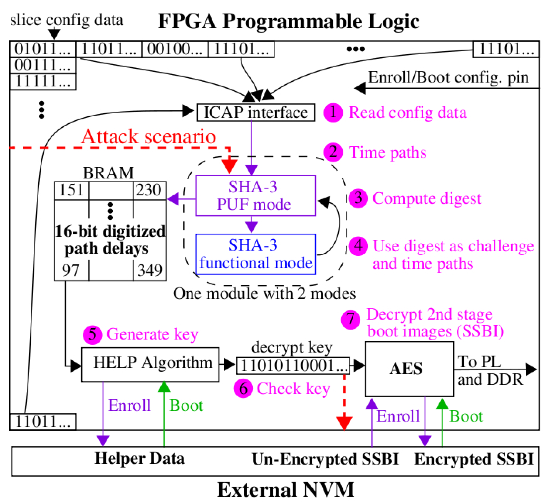
BulletProoF is designed to be self-contained, utilizing only components typically available in the FPGA PL fabric. Specialized, vendor-supplied embedded security components, including E-Fuse, BBRAM, and cryptographic primitives like AES are not used. The BulletProoF boot-up process is illustrated in
Figure 2 as a flow diagram. Similar to the Xilinx boot process, the BootROM loads the FSBL, which then programs the PL side, in this case with the unencrypted BulletProoF bitstream. The FSBL then hands control over to BulletProoF, which carries out some of the functions normally delegated to U-Boot. BulletProoF’s first task is to regenerate the decryption key. It accomplishes this by reading all of the configuration information programmed into the PL side using the ICAP interface [
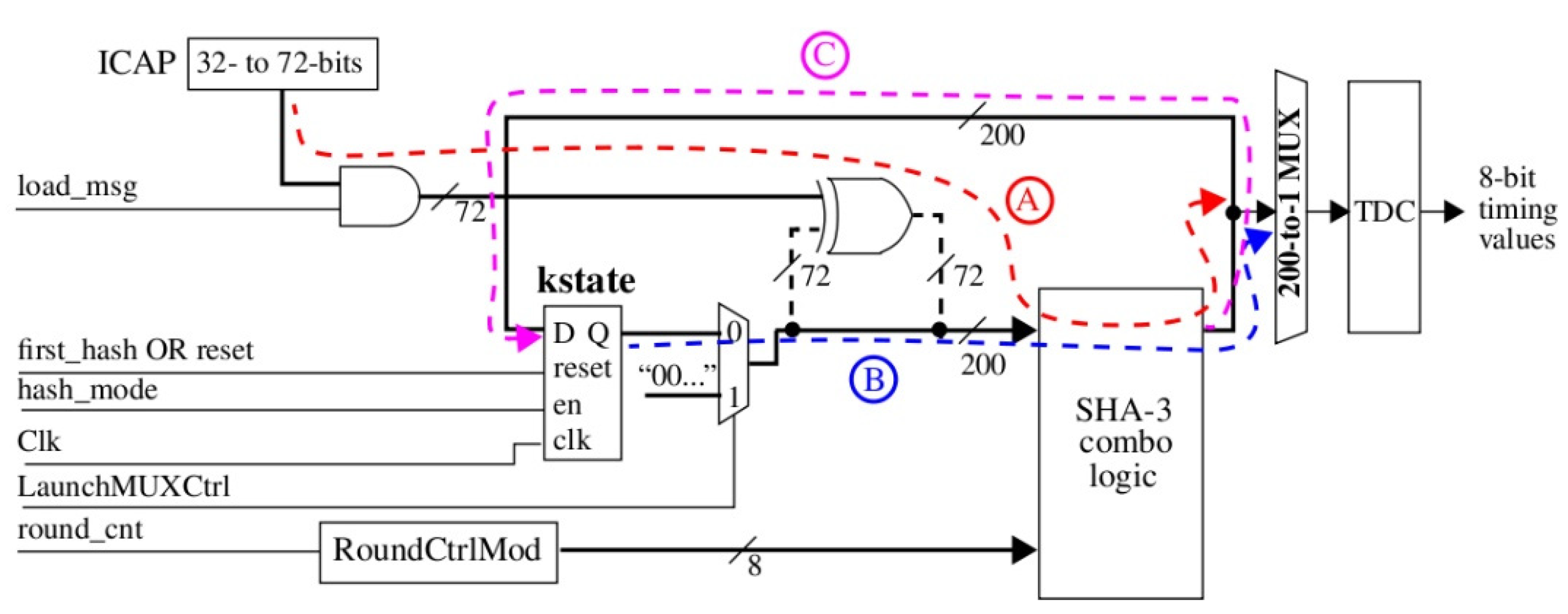
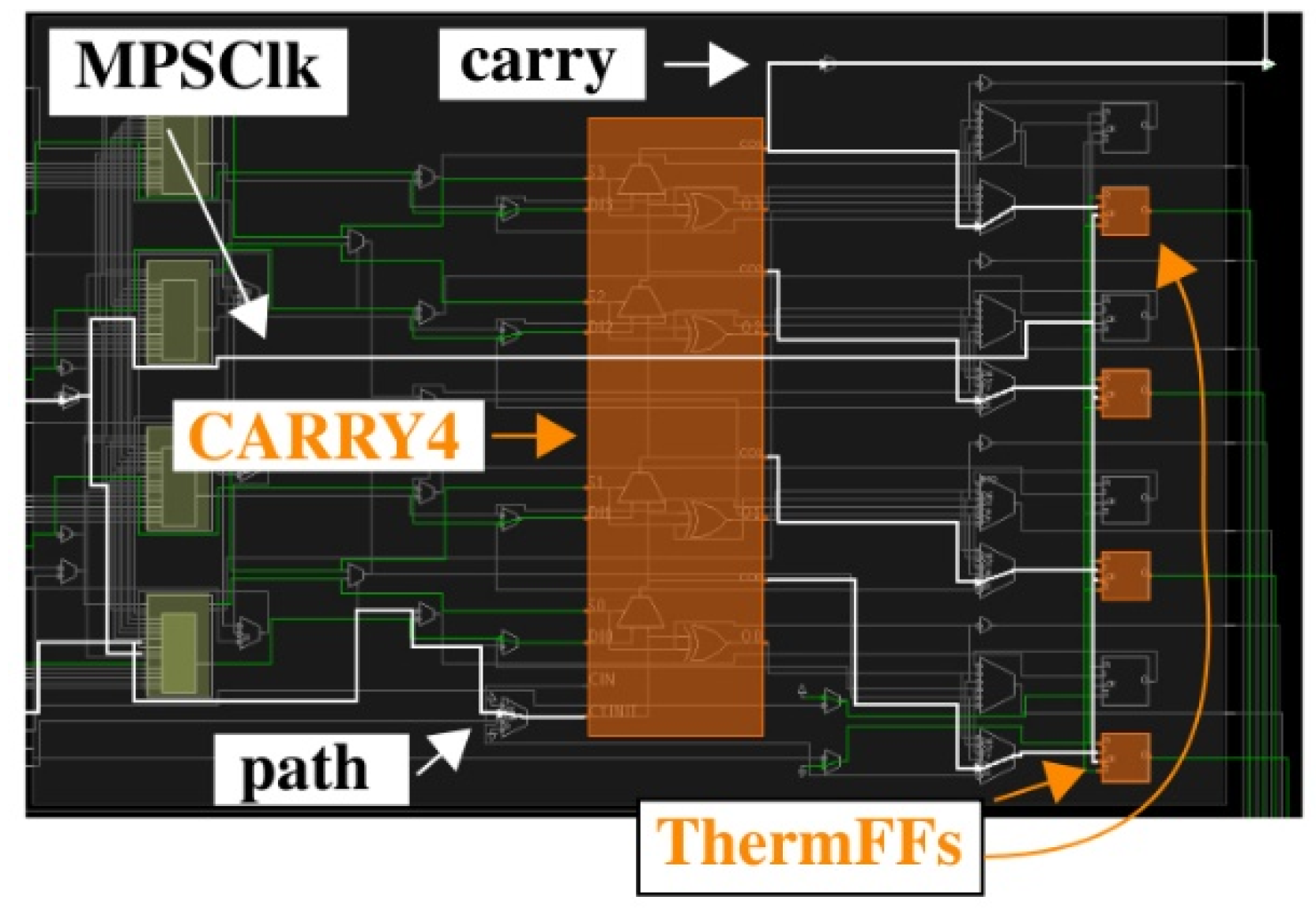
3]. As configuration data is read, it is used as a challenge to time paths between the ICAP and the SHA-3 functional unit (see
Figure 3), and as inputs to the SHA-3 cryptographic hash function to compute a chained set of digests.
As configuration data is read and hashed, BulletProoF periodically changes the mode of SHA-3 from hash mode to a specialized PUF mode of operation. PUF mode configures SHA-3 such that the combinational logic of SHA-3 is used as a source of entropy for key generation. The HELP PUF uses each digest as a challenge to the SHA-3 combinational logic block. HELP measures and digitizes the delays of paths sensitized by these challenges at high resolution and stores them in an on-chip BRAM for later processing. The same timing operation is carried out for paths between the ICAP and SHA-3 outputs, as discussed above, and Field-programmable gate arrays the timing data combined and stored with the SHA-3 timing data in the BRAM. This process continues with additional configuration data added to the existing hash (chained), until all of the configuration data is read and processed.
BulletProoF then reads the externally stored Helper Data and delivers it to the HELP algorithm as needed during the key generation process that follows. The decryption key is transferred to an embedded PL-side AES engine. BulletProoF reads the encrypted second stage boot image components (labeled 3 through 9 in
Figure 2) from the external NVM and transfers them to the AES engine.
An integrity check is performed at the beginning of the decryption process as a mechanism to determine if the proper key was regenerated. The first component decrypted is the key integrity check component (labeled 3 in
Figure 2). This component can be an arbitrary string or a secure hash of, for instance, U-Boot.elf, which is encrypted during enrollment and stored in the external NVM. An unencrypted version of the key integrity check component is also stored as a constant in the BulletProoF bitstream. The integrity of the decryption key is checked by comparing the decrypted version with the BulletProoF version. If they match, then the integrity check passes and the boot process continues. Otherwise, the FPGA is deactivated and the secure boot fails.
If the integrity check passes, BulletProoF then decrypts and authenticates components 4 through 9 in
Figure 2 using 256-bit AES in CBC mode and HMAC, resp., starting with the application (App) bitstream. An application bitstream is programmed into the unused components of the PL side by BulletProoF, using dynamic partial reconfiguration. BulletProoF then decrypts the software components, e.g., Linux, etc. and transfers them to U-Boot. The final step is to bootstrap the processor to start executing the Linux OS (or bare-metal application).
4.1. BulletProoF Enrollment Process
BulletProoF uses a physical unclonable function (PUF) to generate the decryption key, as a mechanism for eliminating the vulnerabilities associated with on-chip key storage. Key generation using PUFs requires an enrollment phase, which is carried out in a secure environment, i.e., before the system is deployed to the field. During enrollment, when the key is generated for the first time, HELP generates the key internally and transfers helper data off of the FPGA. As shown in
Figure 2, the helper data is stored in the external NVM unencrypted. The internally generated key is then used to encrypt the other components of the external NVM (second-stage boot image, or SSBI) by configuring AES in encryption mode.
BulletProoF uses a configuration I/O pin (or an E-Fuse bit) to determine whether it is operating in Enroll mode or Boot mode. The pin is labeled “Enroll/Boot config. pin” in
Figure 3. The trusted party configures this pin to Enroll mode, in order to process the “UnEncrypted SSBI” to an “Encrypted SSBI”, and to create the helper data. The Encrypted SSBI and helper data are stored in an External NVM and later used by the fielded version to boot (see “Enroll” annotations along the bottom of
Figure 3). Therefore, the Enroll and Boot versions of BulletProoF are identical. Note that the “Enroll/Boot config. pin” allows the adversary through board-level modifications, in order to create new versions of the Encrypted SSBI, but the primary goal of BulletProoF, i.e., to protect the confidentiality and integrity of the trusted authority’s second-stage boot image, is preserved.
4.2. BulletProoF Fielded Boot Process
A graphical illustration of the secure boot process carried out by the fielded device is illustrated in
Figure 3. As indicated above, the FSBL loads the unencrypted version of BulletProoF from the external NVM into the PL of the FPGA, and hands over control to BulletProoF. As discussed further below, BulletProoF utilizes a ring oscillator as a clock source that cannot be disabled during the boot process once it is started. This prevents attacks that attempt to stop the boot process at an arbitrary point in order to reprogram portions of the PL using external interfaces, e.g., PCAP, SelectMap, or JTAG. The steps and annotations in
Figure 3 are defined as follows:
BulletProoF reads configuration data using the ICAP interface, using a customized controller.
Every n-th configuration word is used as a challenge to time paths between the ICAP and the SHA-3 outputs with SHA-3 configured in PUF mode (this is done to prevent a specific type of reverse-engineering attack, discussed later.). The digitized timing values are stored in an on-chip BRAM.
The remaining configuration words are applied to the inputs of SHA-3 in functional mode to compute a chained sequence of digests.
Periodically, the existing state of the hash is used as a challenge with SHA-3 configured in PUF mode, to generate additional timing data. The digitized timing values are stored in an on-chip BRAM.
Once all configuration data is processed, the HELP algorithm processes the digitized timing values into a decryption key using helper data, which are stored in an external NVM.
BulletProoF runs an integrity check on the key.
BulletProoF reads the encrypted second-stage boot image (SSBI) from the external NVM. AES decrypts the image and transfers the software components to U-Boot, and the hardware components into the unused portion of the PL, using dynamic partial reconfiguration. Once completed, the system boots.
4.3. Security Properties
The primary goal of BulletProoF is to protect the second-stage boot images, i.e., prevent them from being decrypted, changed, encrypted, and installed back into the fielded system. The proposed system has the following security properties in support of this objective:
The enrollment and regeneration process proposed for BulletProoF never reveals the key outside the FPGA. Therefore, physical, side-channel-based attacks are necessary in order to steal the key. We do not address side-channel attacks in this paper, but it is possible to design the AES engine with side-channel attack resistance using circuit countermeasures, as proposed in [
10].
Any type of tampering with the unencrypted BulletProoF bitstream or helper data by an adversary will only prevent the key from being regenerated, and a subsequent failure of the boot process. Note that it is always possible to attack a system in this fashion, i.e., by tampering with the contents stored in the external NVM, independent of whether it is encrypted or not.
Any attempt to reverse-engineer the unencrypted bitstream, in an attempt to insert logic between the ICAP and SHA-3 input, will change the timing characteristics of these paths, resulting in key regeneration failure. For example, the adversary may attempt to rewire the input to SHA-3, in order to allow external configuration data (constructed to exactly model the data that exists in the trusted version) to be used instead of the ICAP data.
The adversary may attempt to reverse-engineer the helper data to derive the secret key. As discussed in [
11], the PUF used by BulletProoF uses a helper data scheme that does not leak information about the key.
The proposed secure boot scheme stores an unencrypted version of the BulletProoF bitstream, and therefore, adversaries are free to change components of BulletProoF or add additional functionality to the unused regions in the PL. As indicated, changes to configuration data read from ICAP are detected, because the paths that are timed by the modified configuration data are different, which causes key regeneration failure.
BulletProoF uses a ring oscillator as a clock source. Therefore, once BulletProoF is started, it cannot be stopped by the adversary as a mechanism for stealing the key (this attack is elaborated on below).
BulletProoF disables the external programming interfaces (PCAP, SelectMap, and JTAG) prior to starting to prevent adversaries from attempting to perform dynamic partial reconfiguration during the boot process. BulletProoF actively monitors the state of these external interfaces during the boot, and destroys the timing data and keys if any changes are detected.
BulletProoF erases the timing data from the BRAM once the key is generated, and destroys the key once the second-stage boot image is decrypted. The key is also destroyed if the key integrity check fails.
6. Statistical Analysis
The HELP PUF within BulletProoF must be able to regenerate the decryption key without bit-flip errors and without any type of interaction with a server. We propose a bit-flip error avoidance scheme in [
15] that creates three copies of the key, and uses majority voting to eliminate inconsistencies that occur in one of the copies at each bit position. The scheme is identical to traditional triple-modular-redundancy (TMR) methods used in fault tolerance designs. We extend this technique here to allow additional copies, e.g., 5 MR, 7 MR, 9 MR, etc., and combine it with a second reliability-enhancing method, called
margining [
9,
11]. We call the combined method secure-key-encoding (SKE), because the helper data does not leak any information about the secret key. The helper data generated during enrollment is stored in an NVM, and is read during the key regeneration process as discussed earlier, in reference to
Figure 3.
The margining method creates weak bit regions to identify PUF Numbers (PN, from
Figure 7) that have a high probability of generating bit-flip errors. We refer to these PN as unstable, and their corresponding bits as weak. A helper data bitstring is generated during enrollment, which records the positions of the unstable PN in the sequence that is processed. Helper data bits that are 0 inform the enrollment and regeneration key generation process to skip over these PN. On the other hand, the PN classified as stable are processed into key bits, called strong bits. The SKE enrollment process constructs an odd number of strong bit sequences, where each sequence is generated from independent PN but are otherwise identical (redundant) copies of each other. During regeneration, the same sequences are again constructed possibly with bit-flip errors. Majority voting is used to avoid bit-flip errors in the final decryption key, by ignoring errors in 1 of the 3 copies (or 2 of the 5 copies, etc.) that are inconsistent with the bit value associated with the majority. The number of copies is referred to as the
redundancy setting, and is given as 3, 5, 7, etc.
Reference [
11] describes several other features of the HELP algorithm. For example, HELP processes sets of 4096 PN into a multi-bit key, in contrast to other PUFs, which generate key bits one at a time. HELP also includes several other parameters beyond the margin, and the number of redundant copies used in the majority voting scheme just discussed. For example, HELP allows the user to specify a pair of linear feedback shift registers (LFSR) seeds that are then used to pseudo-randomly pair the 4096 PN to create 2048 PN differences. HELP also defines a third reliability-enhancing technique that is based on applying linear transformations to the 2048 PN differences, and includes a modulus operation designed to remove path-length bias effects. The decryption key produced by HELP is dependent on the values assigned to these parameters. It follows, then, that a comprehensive evaluation of bitstring statistical quality requires the analysis to be performed under different parameter combinations.
The statistical results reported here investigate one set of challenges, two margins of 3 and 4, and nine moduli between 14 and 30. The statistics are averaged across 400 groups of 2048 PN differences, created using different LFSR seed pairs. Although this represents only a small portion of the total challenge–response space of HELP, it is sufficiently diverse to provide a good model of the expected behavior under different challenge sets and parameter combinations.
Unlike previously reported statistics on the HELP PUF, the results shown here were generated using the TDC described in
Section 5.2. The three standard statistical quality metrics evaluated included uniqueness (using the inter-chip hamming distance), reliability (using the intra-chip hamming distance), and randomness (using the National Institute of Standards and Technology (NIST) statistical test suite). The analysis was carried out using data collected from a set of 30 Xilinx Zynq 7020 chips (on Zedboards [
16]). The data was collected under enrollment conditions at 25 °C and 1.00 V, and over a set of 15 temperature-voltage (TV) corners represented by all combinations of temperatures (−40 °C, 0 °C, 25 °C, 85 °C, and 100 °C) and voltages (0.95 V, 1.00 V, and 1.05 V).
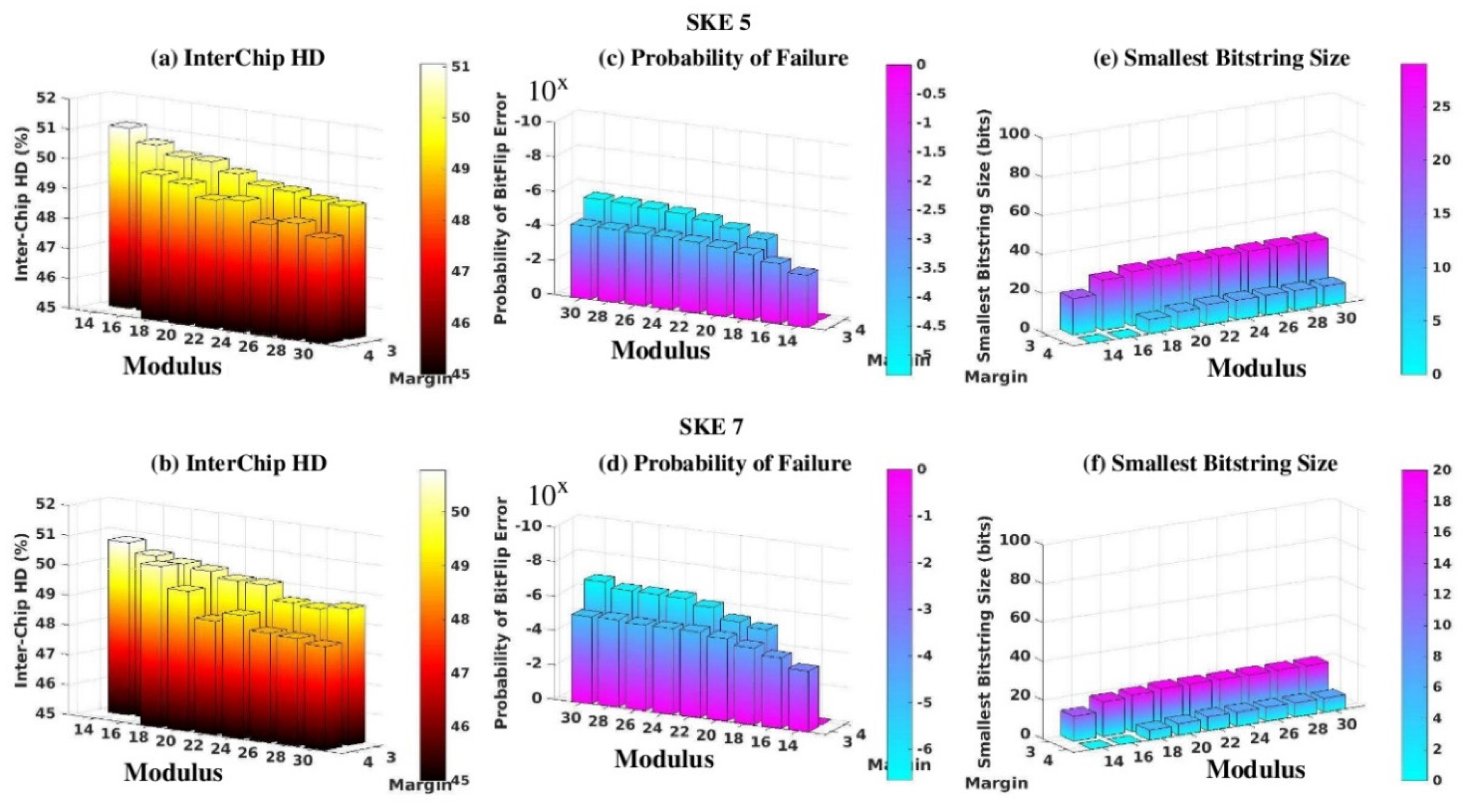
The bar graphs shown in
Figure 8 present the statistical results for the inter-chip hamming distance (HD), in (a) and (b); the probability of failure, in (c) and (d); and the smallest bitstring size in (e) and (f) for SKE, using redundancy settings of 5 (top row) and 7 (bottom row). Here, the final bitstring was constructed by using majority voting across 5 and 7 copies of strong bit sequences, respectively. The results for the nine Moduli and two Margins are shown along the
x- and
y-axes, respectively. As indicated earlier, HELP processes 2048 PN differences at a time, which produces a bitstring of length 2048 bits.
The inter-chip hamming distance (HD) was computed by pairing enrollment bitstrings (of length 2048 bits) under all combinations, and is given by Equation (1). The symbol
NC indicates the number of chips, which is 30 in our experiments, and
NCC indicates the number of chip combinations, which is 30 × 29/2 = 435. The symbol
NBa is the number of bits classified as strong in both bitstrings of the (
i,
j) pair. The subscript (
i, 1,
k) is interpreted as chip
i, TV corner 1 (enrollment), and bit
k. The hamming distance is computed by summing the XOR of the individual bits from the bitstring pair, under the condition that both bits are strong (bit positions that have a weak bit in either bitstring of the pair are skipped). The
HDinter values are computed individually using 400 different LFSR seed pairs, which are averaged and reported in
Figure 8a,b. The bar graph shows near-ideal results with inter-chip HDs between 48% and 51% (ideal is 50%).
The probability of failure results shown in
Figure 8c,d are computed using the HD
intra expression given by Equation (2). Here, bitstrings from the same chip under enrollment conditions are paired with the bitstrings generated under the remaining 15 TV corners. The symbol
NC is the number of chips (30),
NT is the number of TV corners (16), and
NBe is the number of bits classified as strong during enrollment. Note that margining creates a helper data bitstring only during enrollment, which is used to select bits in the enrollment and regeneration bitstrings for the XOR operation. An average HD
intra is computed using the values computed for each of the 400 LFSR seeds. The bar graphs plot the average HD
intra as an exponent to 10
x, where 10
−6 indicates 1 bit-flip error in 1 million bits inspected. The best results are obtained from SKE 7, with a margin of 4 (
Figure 8d), where the probability of failure is <10
−6 for moduli ≥22.
The smallest bitstring size results are plotted in
Figure 8e,f. These results portray the worst-case
NBe values, which is associated with one of the chips from the HD
intra analysis carried out using Equation (2). The smallest bitstring sizes (and the average bitstring sizes, which are not shown) remain relatively constant across moduli, and are in the range of 7–12 bits per set of 2048 PN differences for margin 4, and 20–25 bits for margin 3. Therefore, to generate a 128-bit decryption key, approximately 20 LFSR seed pairs need to be processed, in the worst case.
The NIST statistical test results are not shown in a graph, but are summarized as follows. Unlike the previous analyses, the bitstrings used as input to the NIST software tools are the concatenated bitstrings produced across all 400 seeds for each chip. With 30 chips, NIST requires that at least 28 chips pass the test, for the test to be considered passed overall. The following NIST tests are applicable given the limited size of the bitstrings: Frequency, BlockFrequency, two CumulativeSums tests, Runs, LongestRun, FFT, ApproximateEntropy, and two Serial tests. Most of ApproximateEntropy tests failed by up to 7 chips for SKE 5, margin 3 (all of the remaining tests are passed). For SKE 5, margin 4, all but four of the tests passed, and the fails were only by one chip, i.e., 27 chips passed instead of 28 chips. For SKE 7, all but one test was passed for margins 3 and 4, and the test that failed (LongestRun) failed by one chip.
In summary, assuming that the reliability requirements for BulletProoF are 10
−6, the HELP PUF parameters need to be set to SKE 7 and margin 4, and the modulus should be set to be >20. When these constraints are honored, the inter-chip HD is >48%, and nearly all NIST tests are passed. Decryption key sizes of 128 or larger can be obtained by running the HELP algorithm with 20 or more LFSR seed pairs, or by generating additional sets of 4096 PNs as configuration data is read and processed, as described in
Section 4.


