1. Introduction
Laser treatment with femtosecond pulses (fs) has emerged as a topic of intensive investigation due to the recent advances in femtosecond pulse laser availability. Femtosecond lasers are an effective tool for the precision processing of metals [
1], having multiple advantages over the more conventional nanosecond pulse lasers. Unlike the latter, which create an extended heat-affected zone, femtosecond pulse lasers can provide a very rapid transition from the solid state to vapor or plasma omitting melting and the presence of a liquid phase, with only negligible amounts of heat conducted into the surrounding material [
2].
Femtosecond laser treatment was also shown to lead to an increase in nanohardness of aluminum and its alloys both under vacuum and in an ambient environment. Processing in the ambient environment oxidation leads to the formation of oxide phases. The concentration of oxygen may reach 16% [
3]. Elemental changes in AA2024 with picosecond laser ablation were observed by EDS by Ahuir-Torres et al. [
4].
Another feature of femtosecond laser pulse processing is the possible formation of various self-organized structures. The structures emerging at the micro- and nanoscale modify the properties of surfaces, allowing multiple promising applications. They include the creation of superhydrophobic surfaces on stainless steel [
5], polymers [
6], and silicon [
7], drag reduction [
8], the creation of self-cleaning surfaces [
9], the enhancement of heat transfer [
10], chemical sensing [
11], and the enhancement of light absorption in gold [
12], tungsten, and titanium alloys [
13], sulphur-doped silicon [
14], and aluminum foil [
15]. Possible biological applications include the creation of templates for cellular growth [
16] and the enhancement of the stability of dental prosthetics [
17].
The formation of self-assembled structures such as laser-induced periodic surface structures (LIPSS) and conical microstructures by exposure to ultrashort pulses has been described for metals [
18]. The present work focuses on D16T alloy, the Russian equivalent of AA2024-T4 alloy.
This type of artificially aged Al-Cu alloy is used in aviation because of its attractive mechanical properties (e.g., strength-to-weight ratio) and resistance to mechanical damage.
Near-subwavelength periodic ripples (LIPSS) are commonly referred to as surface self-assembled structures. LIPSS are formed upon the interaction of linearly polarized laser irradiation and solid matter. The incident irradiation is scattered on the random roughness features of the surface, and its interaction with surface-scattered electromagnetic waves and, in some cases, with surface plasmon polaritons leads to inhomogeneous energy absorption. This inhomogeneous energy deposition exhibits strong peaks in the Fourier space and therefore results in the creation of periodic and quasiperiodic structures. Radiation is first absorbed by the electronic system, and then energy is transferred to the lattice [
19].
Various phenomena of thermal, chemical, or hydrodynamical nature occur, leading to the spatially modulated removal and redeposition of material. In the case of pulsed incident radiation, the ripples require multiple pulses to fully form, and the pattern of ultimate structure depends on the number of pulses. Thus, the importance of feedback phenomena should be noted. Several aspects of LIPSS formation remain controversial, as discussed in the general literature [
20].
LIPSS formation on aluminum was reported in the literature for high [
3] and low [
21] fluences, including specifically for aluminum alloy AA2024 [
22].
The formation of conical microstructures in metals at higher fluences is attributed to the contribution of two mechanisms, namely, preferential ablation and the redeposition of nanoparticles stimulated by ablation. Initially, impurities or defects lead to the formation of small (several microns in size) precursor cones at locations where the material is ablated to a lesser extent. Then, precursor cones grow due to the preferential ablation in the surrounding areas. This preferential ablation is caused by two factors. First, the sloped cone edges (forming an angle with the incident beam) have a larger area for the same irradiation fluence, and therefore ablate less. Second, some of the radiation is reflected from the sloped cone edges to the surrounding areas [
18]. This explains the growth of the precursor cones into larger (tens of microns) conical microstructures. The microstructures can even grow above the level of the initial surface due to the redeposition of nanoparticles ablated from furrows between the cones. In the case of the scanning ablation regime, multiple layers of nanoparticles redeposit when the laser beam is moved away, and then are re-melted when the beam returns [
18]. Such structures grow both in height and in width, until two cones meet. Then the cones become linked and grow only upwards, while the furrows between them grow deeper downwards [
23].
A detailed coverage of conical microstructure growth on aluminum and other metals at 800 nm 130 fs laser pulses is provided by Nayak [
24]. More specifically, bump-like microstructures along with maze-like microstructures were observed on AA2024 [
25], and the effects of laser fluence and the number of passes on the roughness and reflectivity of ablated areas were examined [
26].
One can conclude that the complex character of matter-radiation interaction over a wide range of fluences causes versatile surface topological and microchemical modification for commonly used engineering alloys and offers a promising dedicated procedure for advanced surface enhancement. This highlights the importance of rigorous characterization of surface structures using modern techniques such as focused ion beam (FIB) milling and lamella cutting.
The present work is devoted to the focused investigation of D16T alloy, the Russian equivalent of AA2024-T4 alloy. Using non-destructive atomic force microscopy (AFM) and confocal laser profilometry, high resolution SEM, and FIB milling, we systematically investigated the formed LIPSS and conical microstructures reaching 50 µm in size and covered by nanoparticles, which were created as a result of laser treatment using 250 fs pulses of a 1033 nm Yb:YAG laser. We discuss how laser scan patterns can lead to non-uniform profiles and surface structure variations. Internal non-uniformity of the micrometer-sized cones is first investigated at the nanometer scale using fine FIB-SEM observations.
4. Discussion
We believe that the slope of the mean bottom line and the uneven roughness of the treated areas are caused by the influence of redeposited ablated material. Ablated material from the areas exposed to the earlier laser pulses partially redeposits to the areas that are exposed later. This leads to decreased light reflectivity of the latter areas and, as a result, their higher absorption and more intensive further ablation. Moreover, this increases the probability of forming conical microstructures, since the redeposited nanoparticles make the ablation less uniform causing a positive feedback for cone growth in a self-stimulating process. Thus, conical structures starting to grow earlier at the edge of the treated area will have a higher aspect ratio, leading to non-uniform roughness. This effect may be undesirable for engineering applications.
The influence of redeposited ablated material on the formation of conical microstructures was described by Zuhlke et al. [
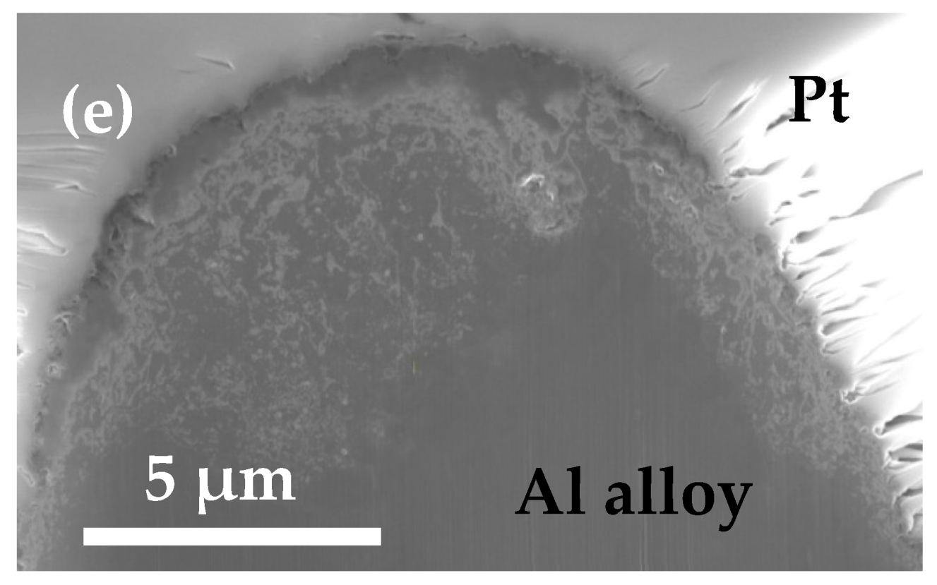
18] in detail. Ablated nanoparticles redeposit when the beam is away, and later, when the scanning beam reaches them again, a portion of the nanoparticles melts. This forms a structure with alternating layers of melted and non-melted particles. The similarity between this work and our work is confirmed when we clearly observe that the conical structures appear to be covered with the layer of sharp nanoparticles, while ultrasonic bath cleaning with acetone removes any loose layer of nanoparticles.
AA2024 that is ablated to the point of conical structure growth has been demonstrated to be a broadband absorber [
26]. We could easily observe this in our work. The low reflectivity can be observed with the naked eye, as the treated areas look black (
Figure 1a). The decrease in reflectivity was approximately evaluated by an integrating sphere measurement. The sphere PVE300 illuminated a spot of 1 mm diameter that was obviously bigger than the width of the treated area; therefore, the signal was collected from both the treated area and the surrounding untreated surface. The untreated alloy’s surface showed a reflectivity of 79 ± 5% in the visible light (300–900 nm) wavelength range, whereas the spot that was positioned in the center of the laser-treated area illuminating both the laser-treated area and the untreated surrounding alloy had an integral reflectivity of 42 ± 2% within the same wavelength range. Applying the linear rule of mixture to the contributions of treated and untreated areas, it was possible to estimate the reflectivity of the treated area as 21 ± 2%.
LIPSS with a 703 nm period were observed on AA2024 in a very recent work for a scan with an 800 fs pulse 1030 nm laser [
22]. Similarly, LIPSS on aluminum are mentioned in the work of Umm-i-Kalsoom et al. [
3]. Those LIPSS were observed at much higher fluences for a treatment conducted using a 30 fs pulse duration and an incident laser wavelength of 800 nm.
Bashir et al. observed LIPSS on Al for low energy fluences, 25 fs pulses, and an 800 nm incident wavelength. The authors concluded that the LIPSS observed were due to the excitation of surface plasmon polaritons and that the period of the structures depended sensitively on the material selected and the laser fluence [
21].
In our work, the LIPSS that we observed were irregular and their period Ʌ seemed to show no dependence on fluence in the range we observed, equaling approximately to 0.73·λ (λ—laser wavelength of 1033 nm). Accordingly, these LIPSS should be attributed to the category of low spatial frequency LIPSS (LSFLs), having a period higher than 0.5·λ. Existing theories explain the formation of LSFLs by the interference of the incident laser pulses and the surface-scattered electromagnetic waves [
20].
A detailed coverage of conical microstructure growth on aluminum and other metals at 800 nm 130 fs laser pulses is presented by Nayak and Gupta [
24]. A focused ion beam (FIB) cutting of a conical structure grown on titanium is provided, with no internal structural change was observed. Conical structures on aluminum exhibited less regularity than the ones created on stainless steel and titanium.
Bump-like microstructures along with maze-like microstructures were observed on AA2024 [
25]. Models were proposed to fine-tune the laser irradiation parameters for the better reproduction of a desired type of microstructure. The differences in the surface structures observed on different metals were explained by differences in the strength of electron-phonon coupling and the thermal conductivities.
Another work providing significant insight into the properties of microstructures grown on AA2024 via femtosecond ablation examines the effect of laser fluence and number of passes on the roughness and reflectivity of ablated areas [
26].
Finally, it is worth mentioning the work revealing the contents of an onion-like aggregated nanoparticle sphere on AA2024 via focused ion beam milling [
27].
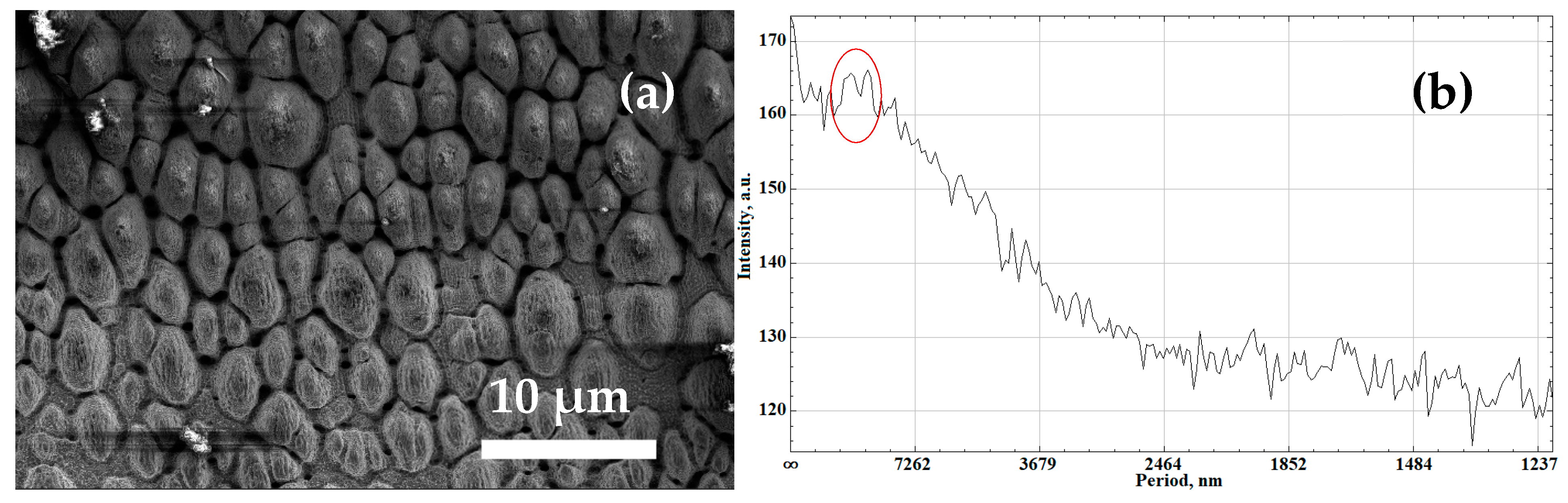
In our case, we supposed that the observed conical structures and deep valleys surrounding them were mostly caused by preferential ablation of lower areas, as described in [
18]. However, while this does define the high aspect ratio of the conical structures for the most part, this is not the only mechanism of structure growth, because profilometry reveals the presence of microstructures higher than the initial surface level. This is most likely caused by the redeposition of ablated material on the cone tops, where less ablation occurs compared to other areas.
While detailed research of conical microstructure growth on AA2024 has already been conducted, to the best of our knowledge, no attempts have been made to study the internal contents of the conical microstructures using FIB-SEM and conducting an EDX study of a lamella cut from the tip of a conical structure. A research paper has conducted an EDX study of the surface of ablated AA2024 [
4]. However, there are significant differences between that work and ours. Exposures were static (no scanning was conducted). In that work, it was shown that more significant elemental change and oxidation were observed at the rim of laser impact and not in the center [
4].
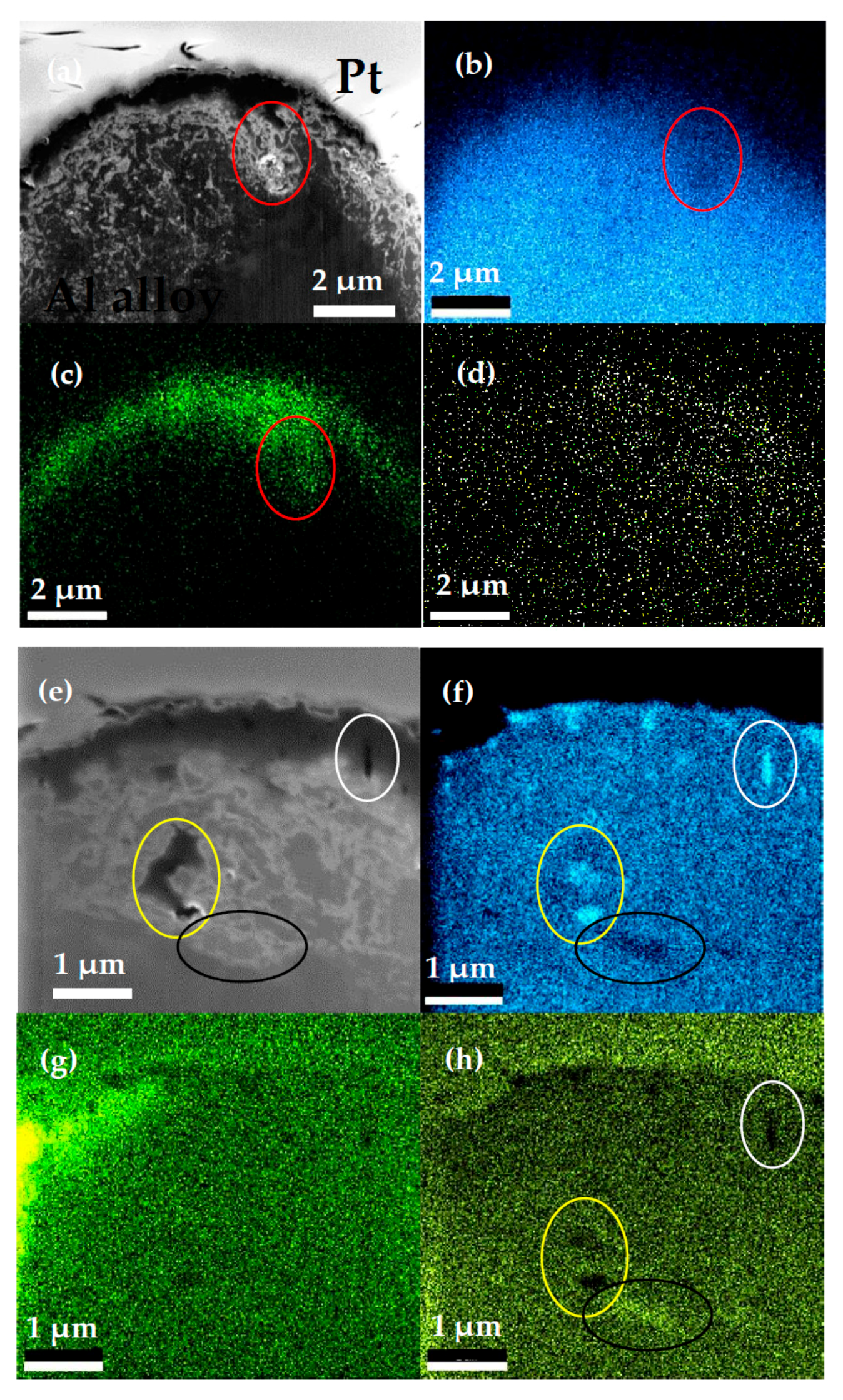
Section 3.4. of this paper provides insight into the structure of the tip of a conical microstructure, grown above the initial surface by redeposition. EDX data reveals the oxidization of treated areas as deep as 3 µm inside the conical microstructures (
Figure 10c). Areas of increased concentration of O and Cu are observed with the respective depletion of Al concentration (
Figure 10b,f), and vice versa. The inhomogeneous distribution of O, Cu, and Al inside the tip can be caused by a number of overlapping possible mechanisms. Stain-like patterns visible inside the lamella cannot be easily explained by changes in elemental concentration or a change in density.
The formation of conical microstructures and LIPSS can be speculatively thought of as dissipative structures similar to Rayleigh-Bénard cells which are formed in non-equilibrium conditions of energy and mass transport within the system. Particular shapes, aspects and sizes of the Rayleigh-Bénard cells are the stationary solutions of parametrical differential equations specific for the particular processing conditions. It can be anticipated that other than conical types of structures formed at laser ablation treatment can be created using the technique presented herein [
28].
Author Contributions
Conceptualization, I.A.S., A.I.S., and A.M.K.; Data curation, I.A.S. and T.F.Y.; Formal analysis, A.I.S. and A.M.K.; Funding acquisition, A.M.K.; Investigation, I.A.S., S.A.L., A.V.N., and T.F.Y.; Methodology, E.S. and A.V.N.; Resources, E.S.; Software, I.A.S. and E.S.; Supervision, S.M., A.I.S., and A.M.K.; Validation, I.S. and A.V.N.; Visualization, I.A.S., S.A.L., I.S., and A.M.K.; Writing—original draft, I.A.S. and A.I.S.; Writing—review and editing, S.M., A.I.S., and A.M.K. All authors have read and agreed to the published version of the manuscript.
Funding
The authors received no external funding.
Acknowledgments
Authors are grateful to Advanced Imaging Core Facility of Skoltech for valuable assistance in FIB-SEM imaging, to M. Chichkov (Shared Facility Center of NUST MISIS, Moscow, Russia) for valuable insight in profilometry, and P.A. Troshin (Center for Energy Science and Technology, Skolkovo Institute of Science and Technology, Moscow, Russia) for useful discussions about AFM data.
Conflicts of Interest
The authors declare no conflict of interest.
References
- Banks, P.S.; Stuart, B.C.; Perry, M.D.; Feit, M.D.; Rubenchik, A.M.; Armstrong, J.P.; Nguyen, H.; Roeske, F.; Lee, R.S.; Myers, B.R.; et al. Femtosecond laser machining. Tech. Dig. Conf. Lasers Electro-Opt. 1998, 6, 510. [Google Scholar]
- Momma, C.; Chichkov, B.N.; Nolte, S.; Alvensleben, F.V.; Tunnermann, A.; Welling, H.; Wellegehausen, B. Short-Pulse laser ablation of solid targets. Opt. Commun. 1996, 129, 134–142. [Google Scholar] [CrossRef]
- Umm-i-Kalsoom; Ali, N.; Bashir, S.; Begum, N.; Rafique, M.S.; Husinsky, W. Morphological, elemental and hardness analysis of femtosecond laser irradiated Al targets. Opt. Laser Technol. 2018, 108, 107–115. [Google Scholar] [CrossRef]
- Ahuir-Torres, J.I.; Arenas, M.A.; Perrie, W.; de Damborenea, J. Influence of laser parameters in surface texturing of Ti6Al4V and AA2024-T3 alloys. Opt. Lasers Eng. 2018, 103, 100–109. [Google Scholar] [CrossRef]
- Wu, B.; Zhou, M.; Li, J. Superhydrophobic surfaces fabricated by microstructuring of stainless steel using a femtosecond laser. Appl. Surf. Sci. 2009, 256, 61–66. [Google Scholar] [CrossRef]
- Nayak, B.K.; Caffrey, P.O.; Speck, C.R.; Gupta, M.C. Superhydrophobic surfaces by replication of micro/nano-Structures fabricated by ultrafast-Laser microtexturing. Appl. Surf. Sci. 2013, 266, 23–32. [Google Scholar] [CrossRef]
- Baldacchini, T.; Carey, J.E.; Zhou, M.; Mazur, E. Superhydrophobic surfaces prepared by microstructuring of silicon using a femtosecond laser. Langmuir 2006, 22, 4917–4919. [Google Scholar] [CrossRef]
- Ahmmed, K.M.T.; Kietzig, A.-M. Drag reduction on laser-Patterned hierarchical superhydrophobic surfaces. Soft Matter 2016, 12, 4912–4922. [Google Scholar] [CrossRef]
- Zorba, V.; Stratakis, E.; Barberoglou, M.; Spanakis, E.; Tzanetakis, P.; Anastasiadis, S.H.; Fotakis, C. Biomimetic artificial surfaces quantitatively reproduce the water repellency of a lotus leaf. Adv. Mater. 2008, 20, 4049–4054. [Google Scholar] [CrossRef]
- Kruse, C.M.; Anderson, T.; Wilson, C.; Zuhlke, C.; Alexander, D.; Gogos, G.; Ndao, S. Enhanced pool-Boiling heat transfer and critical heat flux on femtosecond laser processed stainless steel surfaces. Int. J. Heat Mass Transf. 2015, 82, 109–116. [Google Scholar] [CrossRef]
- Li, G.; Lu, Y.; Wu, P.; Zhang, Z.; Li, J.; Zhu, W.; Hu, Y.; Wu, D.; Chu, J. Fish scale inspired design of underwater superoleophobic microcone arrays by sucrose solution assisted femtosecond laser irradiation for multifunctional liquid manipulation. J. Mater. Chem. A 2015, 3, 18675–18683. [Google Scholar] [CrossRef]
- Vorobyev, A.Y.; Guo, C. Enhanced absorptance of gold following multipulse femtosecond laser ablation. Phys. Rev. B 2005, 72, 195422. [Google Scholar] [CrossRef] [Green Version]
- Vorobyev, A.Y.; Guo, C. Black metals through femtosecond laser pulses. In AIP Conference Proceedings; AIP: College Park, MD, USA, 2012; Volume 1464, p. 397. [Google Scholar]
- Crouch, C.H.; Carey, J.E.; Shen, M. Infrared absorption by sulfur-Doped silicon formed by femto second laser irradiation. Appl. Phys. A 2004, 79, 1635–1641. [Google Scholar] [CrossRef]
- Hwang, T.Y.; Vorobyev, A.Y.; Guo, C. Enhanced efficiency of solar-Driven thermoelectric generator with femtosecond lasertextured metals. Opt. Express 2011, 19, A824. [Google Scholar] [CrossRef] [PubMed]
- Straub, M.; Uchugonova, A.; Koch, M.; König, K. Silicon cell culture templates with nanotopography: Periodic nanostructures and random nanoporous topologies generated by high-Repetition rate sub-15 fs pulsed nearinfrared laser light. Proc. SPIE-Int. Soc. Opt. Eng. 2012. [Google Scholar] [CrossRef]
- Orazi, L.; Maksym, P.; Deineka, V.; Husak, E.; Korniienko, V.; Mishchenko, O.; Reggiani, B. Osteoblast Cell Response to LIPSS-Modified Ti-Implants. Key Eng. Mater. 2019, 813, 322–327. [Google Scholar] [CrossRef]
- Zuhlke, C.A.; Troy, P.A.; Dennis, R.A. Fundamentals of layered nanoparticle covered pyramidal structures formed on nickel during femtosecond laser surface interactions. Appl. Surf. Sci. 2013, 283, 648–653. [Google Scholar] [CrossRef]
- Sipe, J.E.; Young, J.F.; Preston, J.S.; Van Driel, H.M. Laser-Induced periodic surface structures. I. Theory. Phys. Rev. B 1983, 27, 1141–1154. [Google Scholar] [CrossRef]
- Bonse, J.; Hohm, S.; Kirner, S.V.; Rosenfeld, A.; Kruger, J. Laser-Induced Periodic Surface Structures-A Scientific Evergreen. IEEE J. Sel. Top. Quantum Electron. 2017, 23, 9000615. [Google Scholar] [CrossRef]
- Bashir, S.; Rafique, M.S.; Husinsky, W. Femtosecond laser-Induced subwavelength ripples on Al, Si, CaF2 and CR-39. Nucl. Instrum. Methods B 2012, 275, 1–6. [Google Scholar] [CrossRef]
- Zhanga, H.Z.; Wanga, H.Y.; Liub, F.F.; Wangc, L. Investigation on femtosecond laser ablative processing of SiCp/AA2024 composites. J. Manuf. Proc. 2020, 49, 227–233. [Google Scholar] [CrossRef]
- Li, Y.; Cui, Z.; Wang, W.; Lin, C.; Tsai, H.-L. Formation of linked nanostructure-textured mound-shaped microstructures on stainless steel surface via femtosecond laser ablation. Appl. Surf. Sci. 2013, 324, 775–783. [Google Scholar] [CrossRef]
- Nayak, B.K.; Gupta, M.C. Self-Organized micro/nano structures in metal surfaces by ultrafast laser irradiation. Opt. Lasers Eng. 2010, 48, 940–949. [Google Scholar] [CrossRef]
- Tanvir Ahmmed, K.M.; Jee Yang Ling, E.; Servio, P.; Kietzig, A.-M. Introducing a new optimization tool for femtosecond laser-Induced surface texturing on titanium, stainless steel, aluminum and copper. Opt. Lasers Eng. 2015, 66, 258–268. [Google Scholar] [CrossRef]
- Singh, N.; Alexander, D.R.; Schiffern, J.; Doerr, D. Femtosecond laser production of metal surfaces having unique surface structures that are broadband absorbers. J. Laser Appl. 2006, 18, 242–244. [Google Scholar] [CrossRef]
- Tsubaki, T.A.; Kotenb, M.A.; Lucis, M.J.; Zuhlke, C.; Ianno, N.; Shield, J.E.; Alexander, D.R. Formation of aggregated nanoparticle spheres through femtosecond laser surface processing. Appl. Surf. Sci. 2017, 419, 778–787. [Google Scholar] [CrossRef] [PubMed] [Green Version]
- Khmelevskaya, V.S.; Malynkin, V.G. Anomalous states in metallic alloys induced by irradiation. Phase Trans. 1997, 60, 59–65. [Google Scholar] [CrossRef]
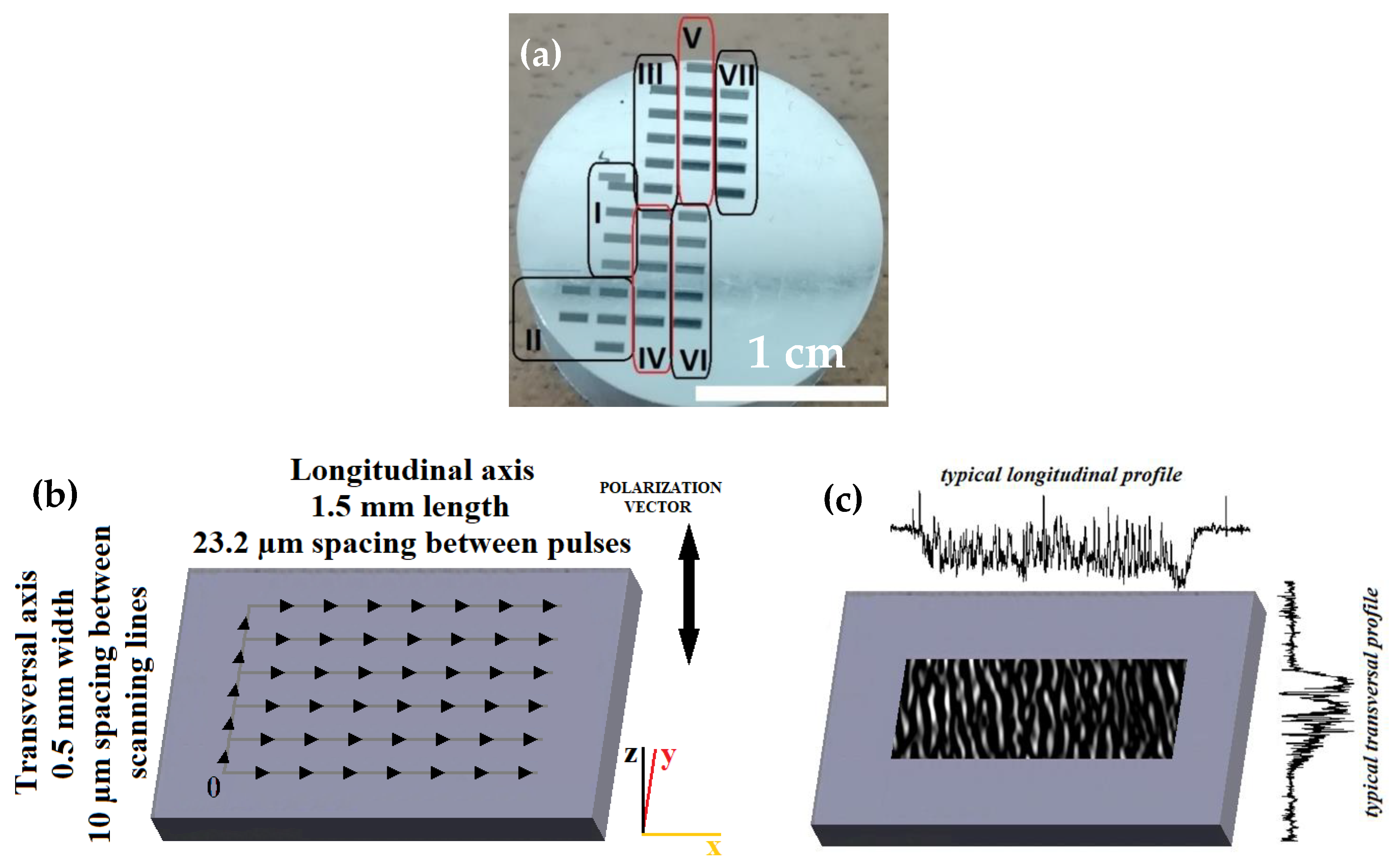
Figure 1.
Layout and principal geometry characteristics of laser treatment: (a) photograph of cylindrical D16T sample, with series of treated areas marked; (b) laser scan schematic diagram, with axes defined and scanning (long arrows) and scan progression (short arrows) directions; (c) typical treated area schematic, with laser-induced periodic surface structure LIPSS direction indicated and typical profiles shown.
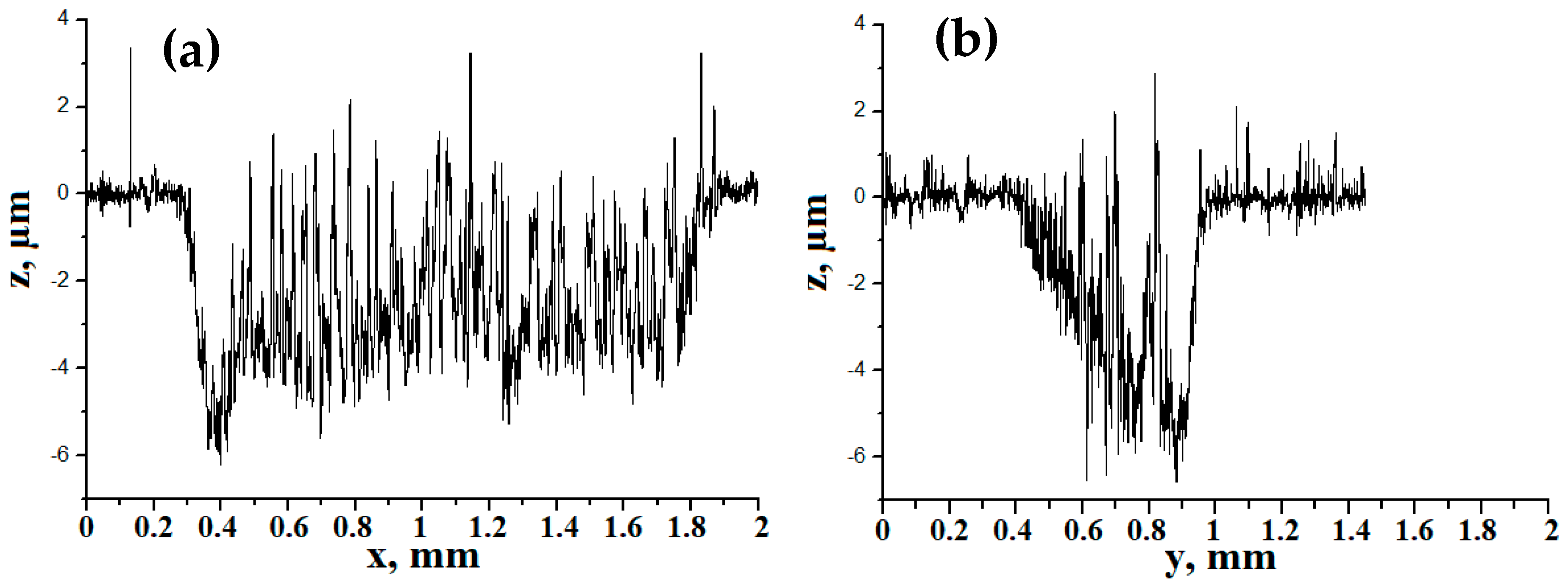
Figure 2.
Typical ablation profiles for 21 J/cm2. The area with three scan repetitions (SR) was chosen for representation: (a) longitudinal profile of treated area bottom; (b) transversal profile of treated area bottom.
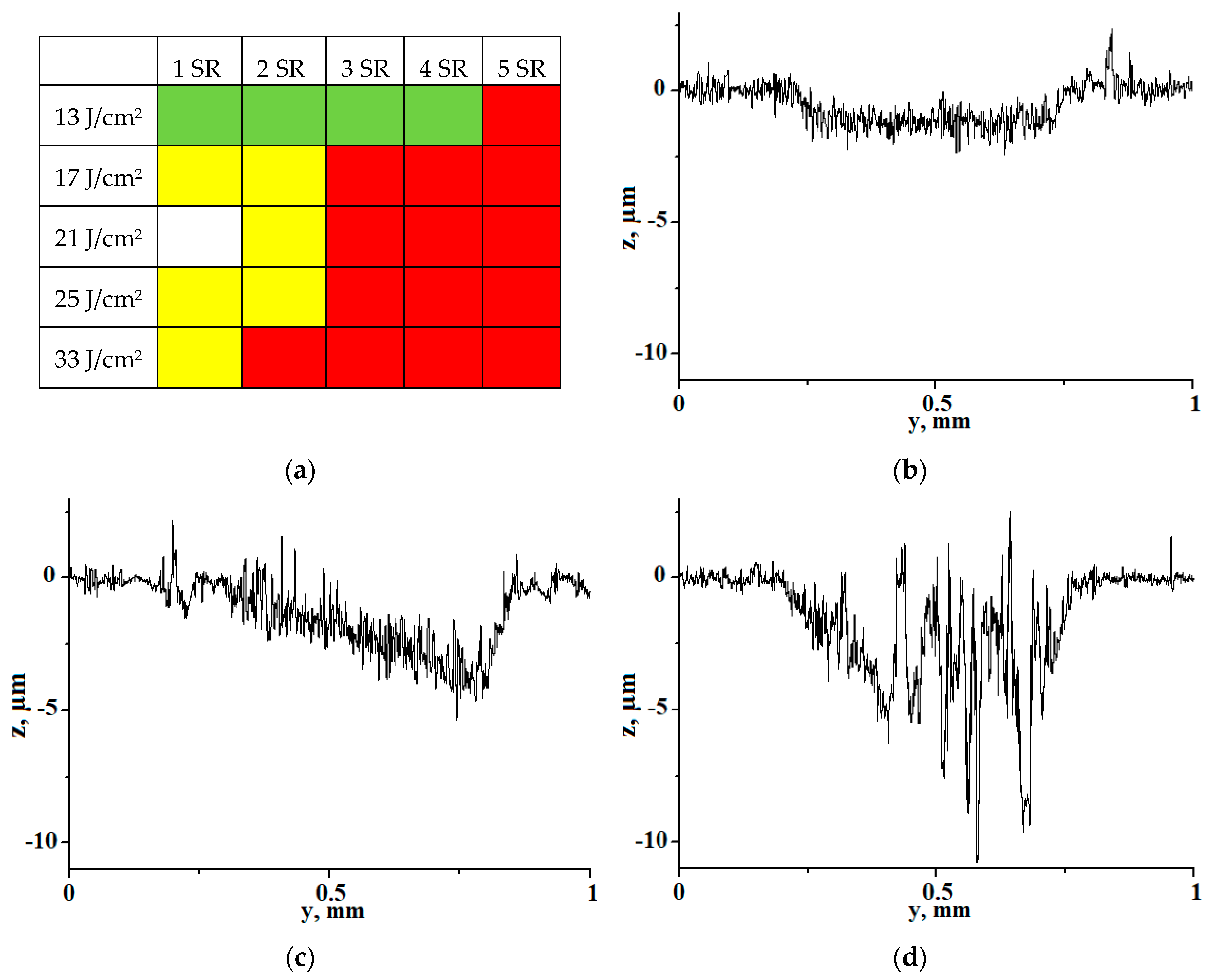
Figure 3.
Profiles of laser-treated areas: (a) color-coded chart; (b) example profile for “green” profiles which are parallel to the initil surface; (c) example profile for “yellow” profiles with an observable slope; (d) example profile for “red” profiles with high roughness. SR: scan repetition.
Figure 4.
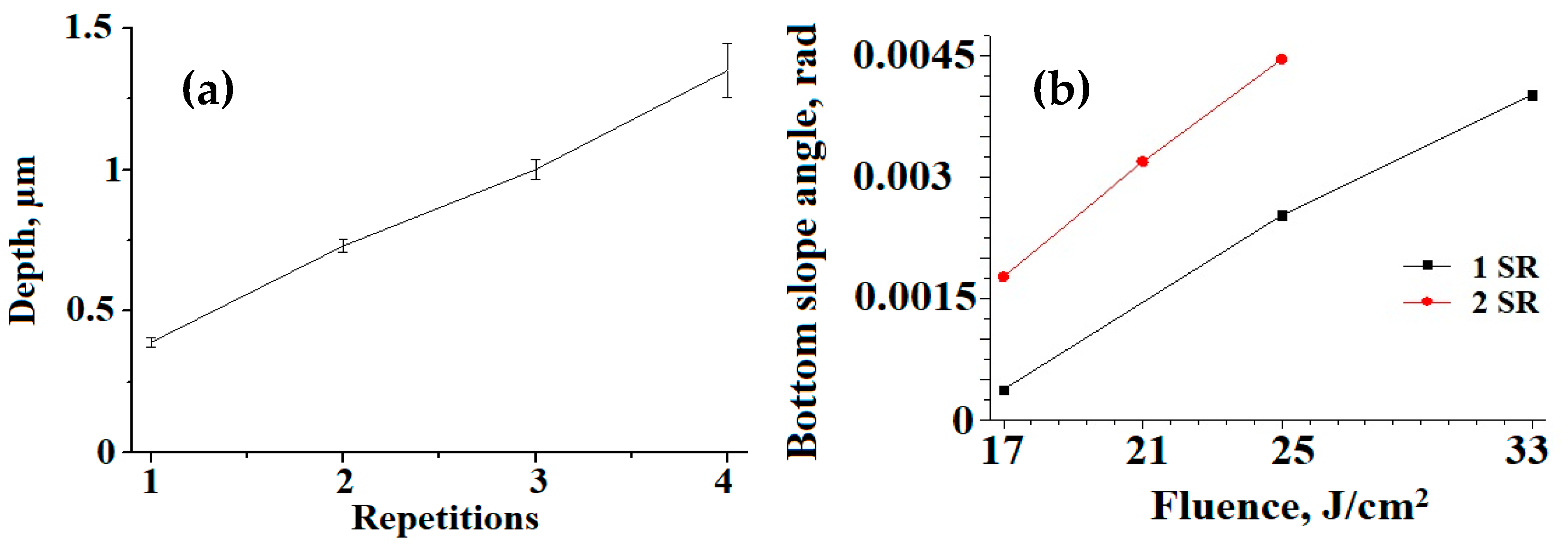
Profile parameters: (a) depth of laser-treated areas at 160 µJ; (b) average slope angle of treated area bottom.
Figure 5.
Appearance of laser-treated areas.
Figure 6.
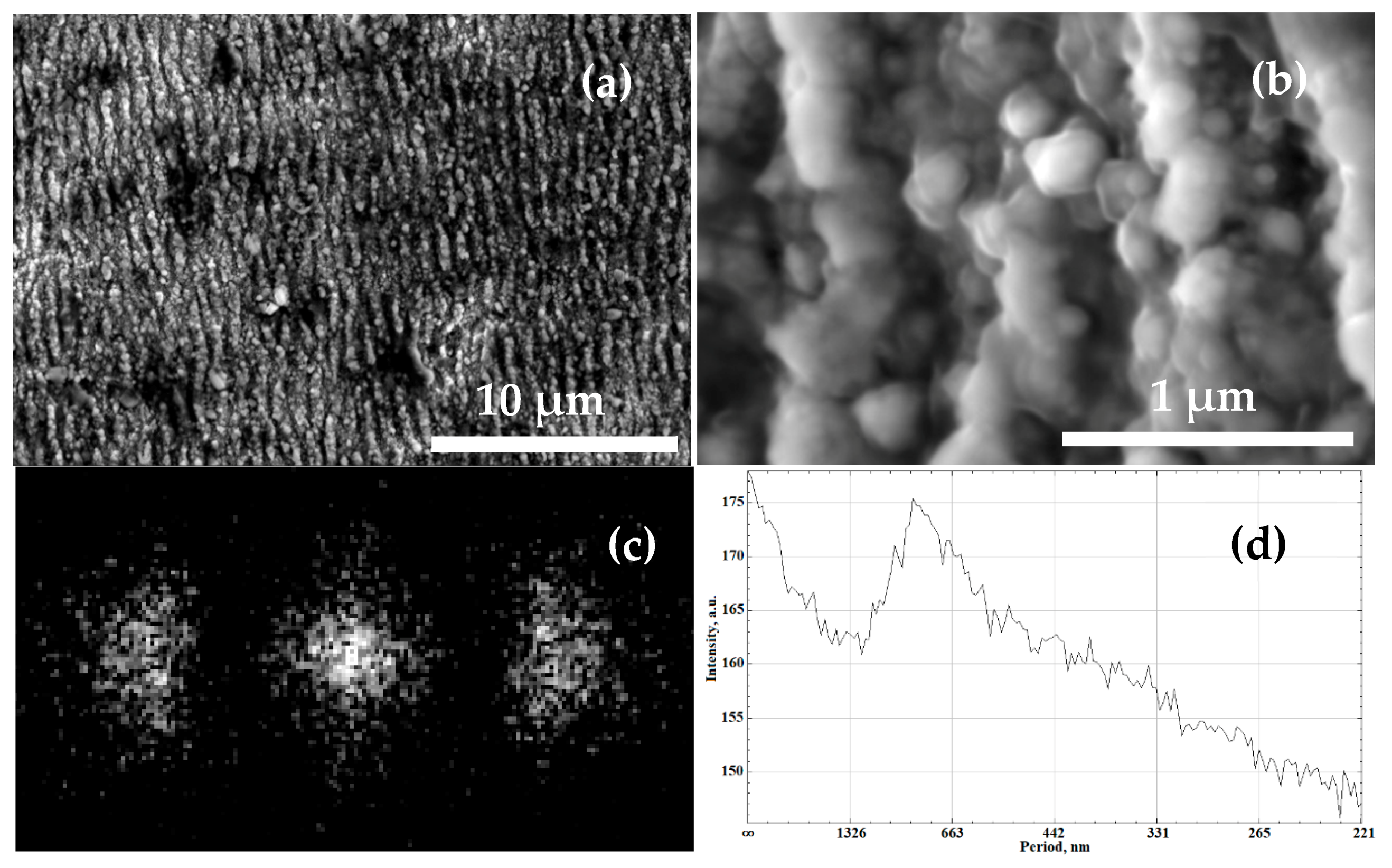
SEM images for 9 J/cm2 with five scan repetitions. (a) Wide shot SEM demonstrating periodic yet loosely regular LIPSS; (b) SEM close-up on LIPSS, revealing a granular structure (observed with 52° sample tilt); (c) FFT of initial SEM image with contrast enhanced; (d) FFT spectrum with the peak clearly visible.
Figure 7.
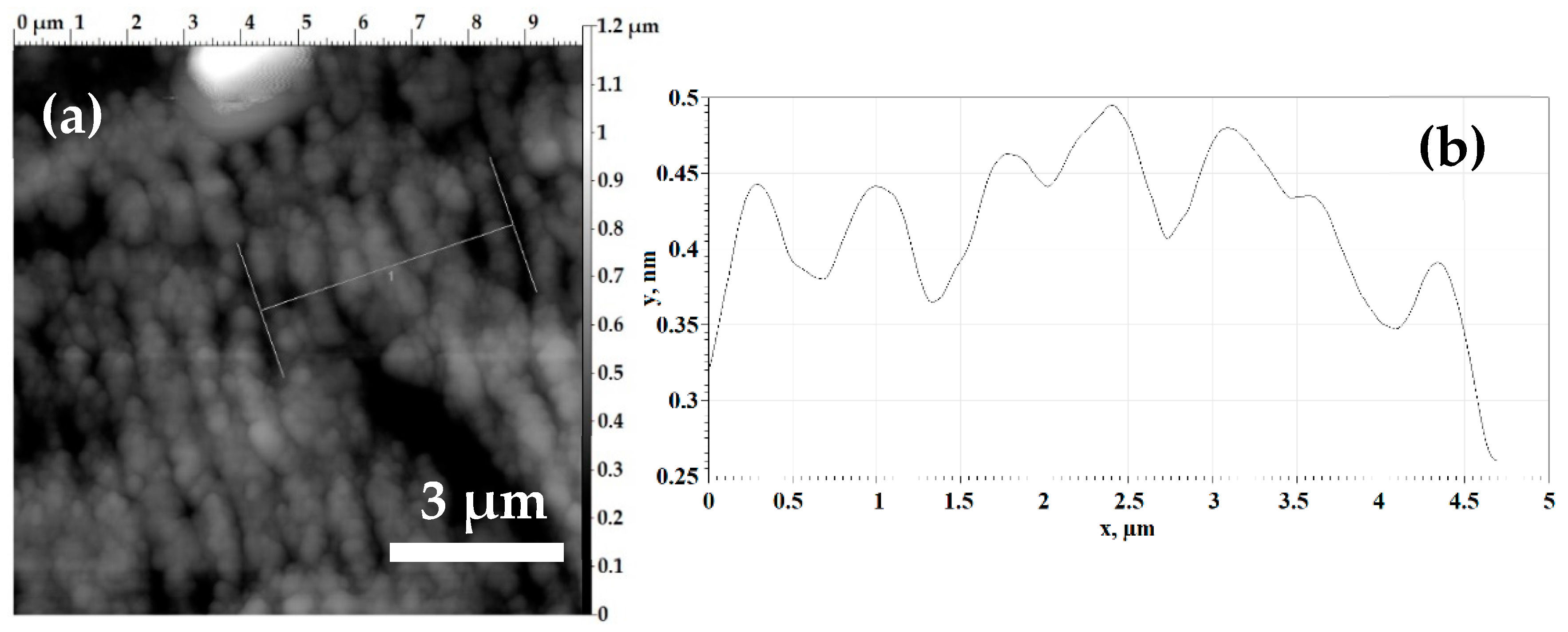
AFM profiling of LIPSS for 5 J/cm2 with three scan repetitions: (a) topography image of a 10 × 10 µm2 area; (b) linear profile along a direction perpendicular to the LIPSS (dashed line).
Figure 8.
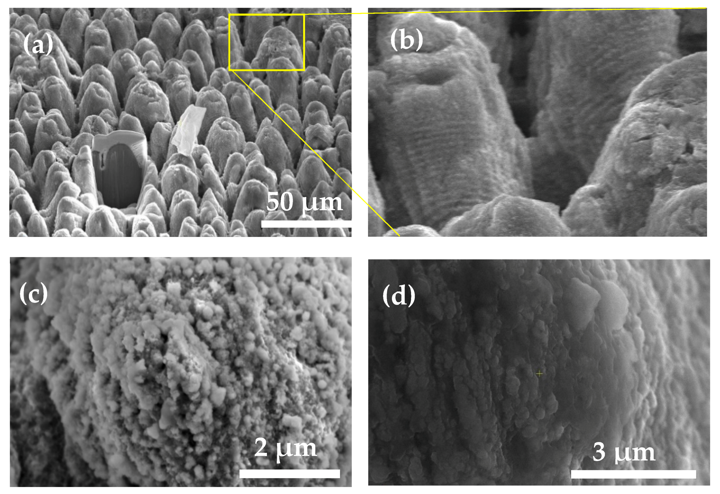
SEM images of conical microstructures for 33 J/cm2 with five scan repetitions: (a) conical microstructures (observed with 52° sample tilt), with an impurity particle and the site of FIB milling; (b) close-up of the conical structures’ slopes with the contrast enhanced, ripples are observable (observed with 52° sample tilt); (c) tip of a conical microstructure before cleaning in acetone; (d) slope of a conical microstructure after cleaning in acetone; (e) internal content of a conical structure sectioned in half by FIB (observed with 52° sample tilt), a protective layer of platinum is deposited on top.
Figure 9.
Image analysis for conical microstructures for 21 J/cm2 with five scan repetitions: (a) SEM image with conical microstructures; (b) fourier transform graph with a peak corresponding to the average conical structure size marked in red.
Figure 10.
FIB sectioning of a cone formed by laser ablation treatment at 33 J/cm2 with five scan repetitions: (a) SEM image of FIB-cut conical structure; (b) EDX showing Al concentration inside the FIB-cut conical structure; (c) EDX showing O concentration inside the FIB-cut conical structure; (d) EDX showing Cu concentration inside the FIB-cut conical structure; (e) SEM image of lamella cut from the conical structure; (f) EDX showing Al concentration inside the lamella cut from the conical structure; (g) EDX showing O concentration inside the lamella cut from the conical structure; (h) EDX showing Cu concentration inside the lamella cut from the conical structure. Contrast is enhanced for all images.
Table 1.
D16T elementary composition.
| D16T (AA2024-T4) | Weight % |
|---|
| Al | Balance |
| Cu | 4.239 ± 0.073 |
| Mg | 1.754 ± 0.037 |
| Mn | 0.532 ± 0.0044 |
| Fe | 0.346 ± 0.011 |
| Si | 0.223 ± 0.0057 |
| Zn | 0.152 ± 0.00071 |
| Ti | 0.047 ± 0.001 |
| Cr | 0.016 ± 0.001 |
Table 2.
Laser beam spot parameters for different treatment series.
| Treatment Series | Pulse Energy, µJ | Energy Fluence, J/cm2 |
|---|
| I | 60 | 5 |
| II | 110 | 9 |
| III | 160 | 13 |
| IV | 210 | 17 |
| V | 260 | 21 |
| VI | 310 | 25 |
| VII | 400 | 33 |
Table 3.
Ra roughness parameter for laser-treated areas, nm.
| Fluence, J/cm2 | 1 Scan Repetitions | 2 Scan Repetitions | 3 Scan Repetitions | 4 Scan Repetitions | 5 Scan Repetitions |
|---|
| 13 | 249 | 219 | 242 | 310 | 744 |
| 17 | 237 | 247 | 412 | 1146 | 773 |
| 21 | 300 | 413 | 661 | 793 | 1423 |
| 25 | 364 | 395 | 598 | 1302 | 1541 |
| 33 | 381 | 735 | 1666 | 1132 | 1133 |
Table 4.
Rz roughness parameter for laser-treated areas, µm.
| Fluence, J/cm2 | 1 Scan Repetitions | 2 Scan Repetitions | 3 Scan Repetitions | 4 Scan Repetitions | 5 Scan Repetitions |
|---|
| 13 | 4.5 | 3.8 | 3.2 | 6.7 | 14.3 |
| 17 | 4.5 | 2.8 | 8.0 | 12.1 | 9.5 |
| 21 | 2.8 | 6.8 | 8.1 | 13.0 | 18.8 |
| 25 | 6.4 | 4.6 | 8.6 | 20.6 | 18.2 |
| 33 | 4.3 | 7.1 | 23.0 | 16.7 | 18.3 |
Table 5.
Period and height of LIPSS per fluence.
| Fluence, J/cm2 | Number of Repeats | LIPSS Period, µm | LIPSS Height, nm |
|---|
| 5 | 3 | 0.8 ± 0.09 | 83.0 ± 14.5 |
| 5 | 5 | 0.8 ± 0.07 | 116.8 ± 24.9 |
Table 6.
Average distance between cone tops per fluence.
| Fluence, J/cm2 | Number of Repeats | Conical Microstructures’ Average Distance, µm |
|---|
| 21 | 5 | 11.55 ± 3.91 |
| 25 | 5 | 18.46 ± 2.21 |
| 33 | 5 | 15.43 ± 3.86 |
© 2020 by the authors. Licensee MDPI, Basel, Switzerland. This article is an open access article distributed under the terms and conditions of the Creative Commons Attribution (CC BY) license (http://creativecommons.org/licenses/by/4.0/).

 ,
, 


