Article

Preparation of Tin Oxide Quantum Dots in Aqueous Solution and Applications in Semiconductor Gas Sensors

1
College of Information Science and Technology, Dalian Maritime University, Dalian 116026, China
2
Department of Material Science and Engineering, Dalian Maritime University, Dalian 116026, China
*
Author to whom correspondence should be addressed.
Submission received: 20 January 2019 / Revised: 1 February 2019 / Accepted: 7 February 2019 / Published: 11 February 2019
(This article belongs to the Special Issue Preparation, Characterization and Utility of Quantum Dots)

Abstract

:
Tin oxide quantum dots (QDs) were prepared in aqueous solution from the precursor of tin dichloride via a simple process of hydrolysis and oxidation. The average grain size of QDs was 1.9 nm. The hydrothermal treatment was used to control the average grain size, which increased to 2.7 and 4.0 nm when the operating temperatures of 125 and 225 °C were employed, respectively. The X-ray photoelectron spectroscopy (XPS) spectrum and X-ray diffraction analysis (XRD) pattern confirmed a rutile SnO2 system for the QDs. A band gap of 3.66 eV was evaluated from the UV-VIS absorption spectrum. A fluorescence emission peak was observed at a wavelength of 300 nm, and the response was quenched by the high concentration of QDs in the aqueous solution. The current-voltage (I-V) correlation inferred that grain boundaries had the electrical characteristics of the Schottky barrier. The response of the QD thin film to H2 gas revealed its potential application in semiconductor gas sensors.

1. Introduction

The semiconductor quantum dot (QD) is a very small three-dimensional system with dimensions of several nanometers. It is constituted by a few hundred atoms, much fewer than the atom number of a bulk system. Because of the small size of QDs, the energy states for electrons, holes, and excitons are discrete series, revealing the effect of quantum confinement. They bring unique characteristics that are valuable for producing advantageous electronic devices. Thus, in recent decades, QDs have attracted a lot of attention. For example, Alberto prepared PbS QDs for photoconductors, in which the control of surface chemistry offered a direct approach for the tuning of charge carrier dynamics based on strongly coupled QD solids [1]. Ternary alloy PbCdS QDs were explored as photosensitizers for quantum dot sensitized solar cells [2]. CdSe QDs were used as ultrasensitive sensors for Pb2+ heavy metal ions [3] and fluorescent nanomarkers for diesel oil [4]. Colloidal QDs of PbS, ZnO, and WO3 were good candidates for novel semiconductor gas sensors [5,6,7,8,9]. Even though the semiconductor QDs of CdSe, PbS, and CdS showed perspectives in the practical applications, their toxicities have to be considered. The elements of cadmium, lead, and telluride have been proved to be harmful to many kinds of living things, especially after their accumulation through the food web [10].
Tin oxide (SnO2) is a classical semiconductor, which has a wide direct band gap of 3.6 eV. It holds the advantages of good chemical stability, non-toxicity, and low cost. Recently, dozens of works have been published to report the applications of SnO2 QDs in novel electronic devices of gas sensors [11,12,13,14,15,16,17], photocatalysts [18,19], solar cells [20,21], and lithium-ion batteries [22,23]. Many techniques have been developed to prepare QD elements and devices, such as molecular beam epitaxy, metal-organic chemical vapor deposition, and some chemical routes [24]. However, these methods relied on complex facilities, or included organic compounds, which may bring potential toxicity to human beings or the environment. For example, SnO2 QDs were synthesized via a solvothermal route, in which organic reagents of oleic acid, oleylamine, and toluene were used [25,26]. Bathula prepared SnO2 QDs from the precursor of tin chloride pentahydrate with the aid of hydrazine and ethanol [27]. The consumption of toxic organics in the QD fabrication process not only put employees in danger but also increased the cost in environmental remediation by factories. Therefore, a simple and cheap method to prepared SnO2 QDs is expected.
In the present work, SnO2 QDs were prepared in aqueous solution via a simple route of hydrolysis and oxidation of SnCl2·2H2O, with the catalytic of CH4N2S. The hydrothermal treatment was introduced to control the grain growth of QDs. The characteristics of composition, morphology, grain size, photonic adsorption, fluorescence spectrum, and electrical property were concluded for the prepared QDs.

2. Materials and Methods
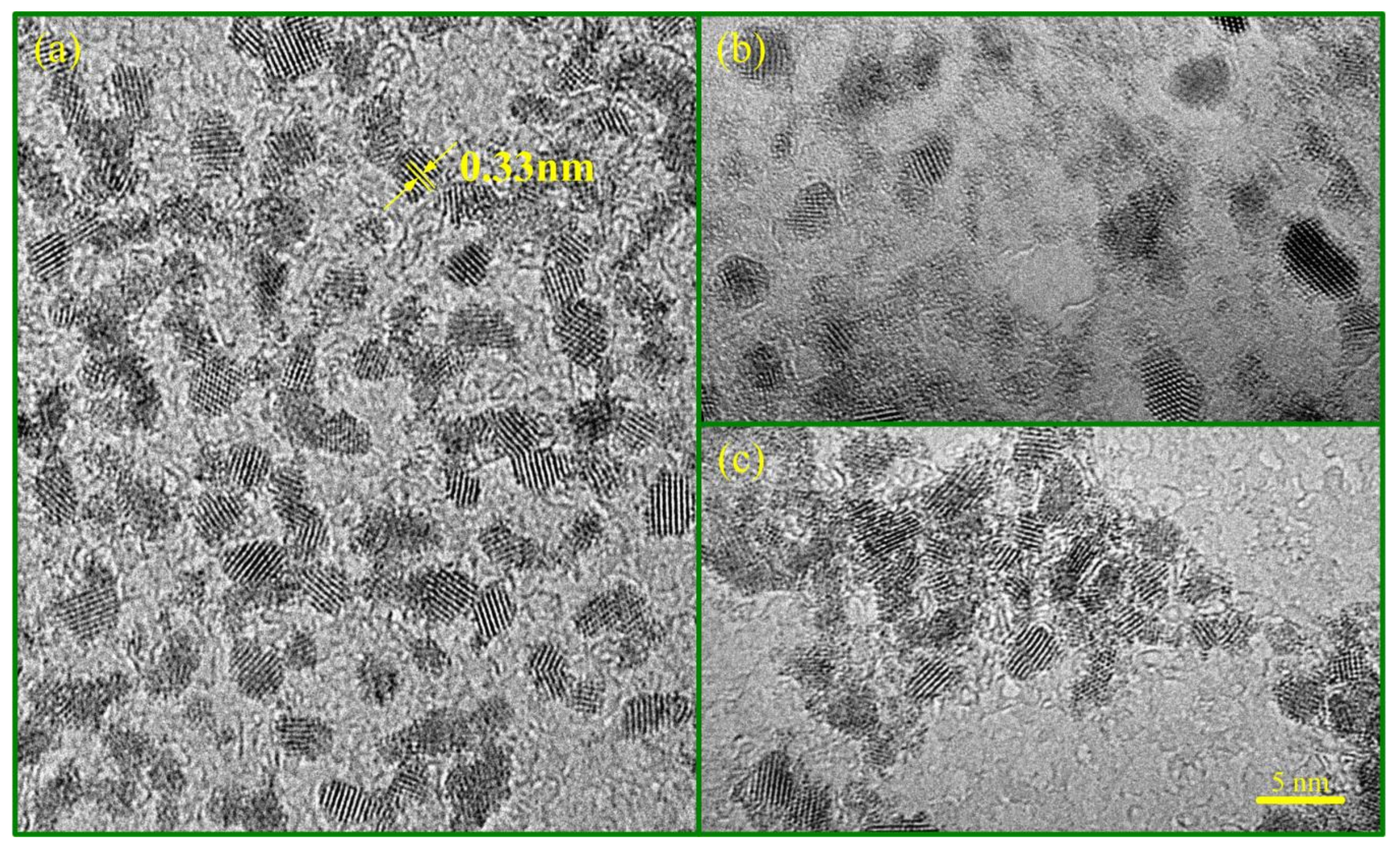
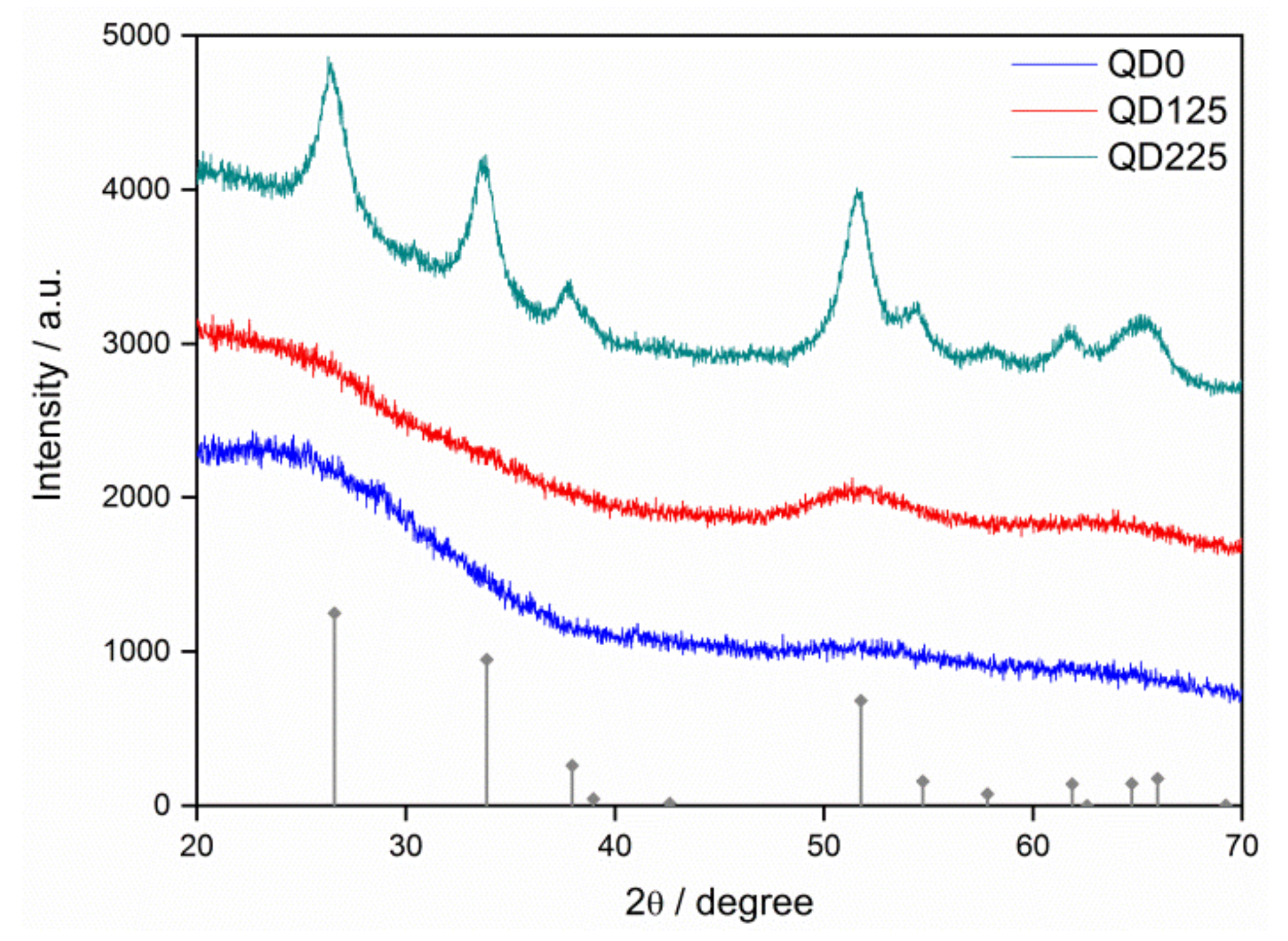
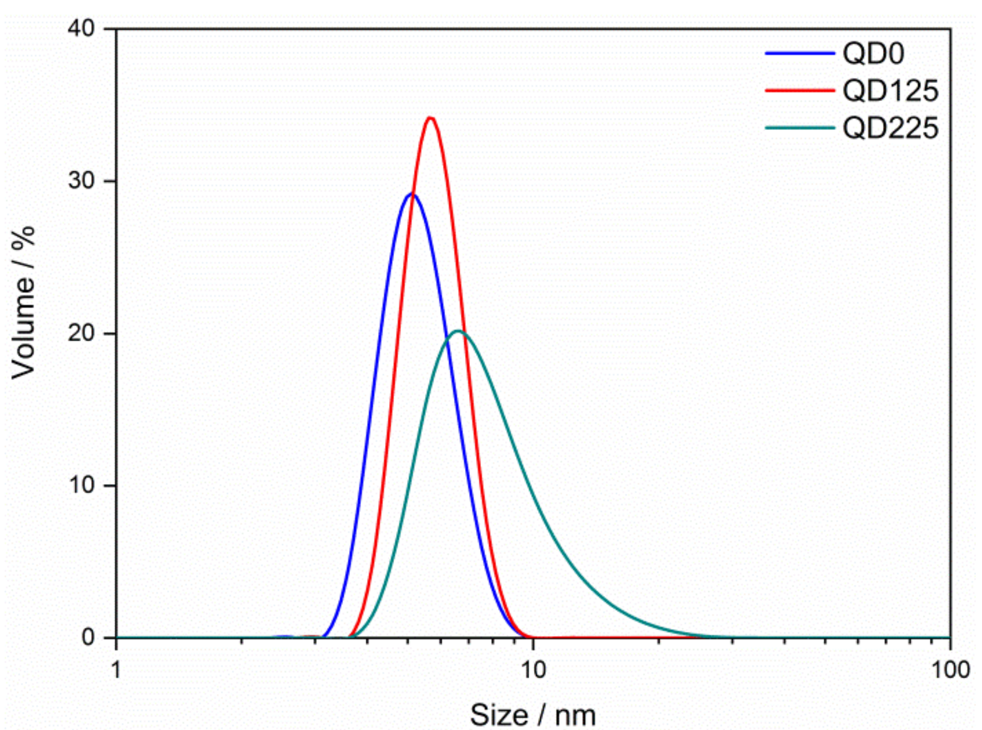
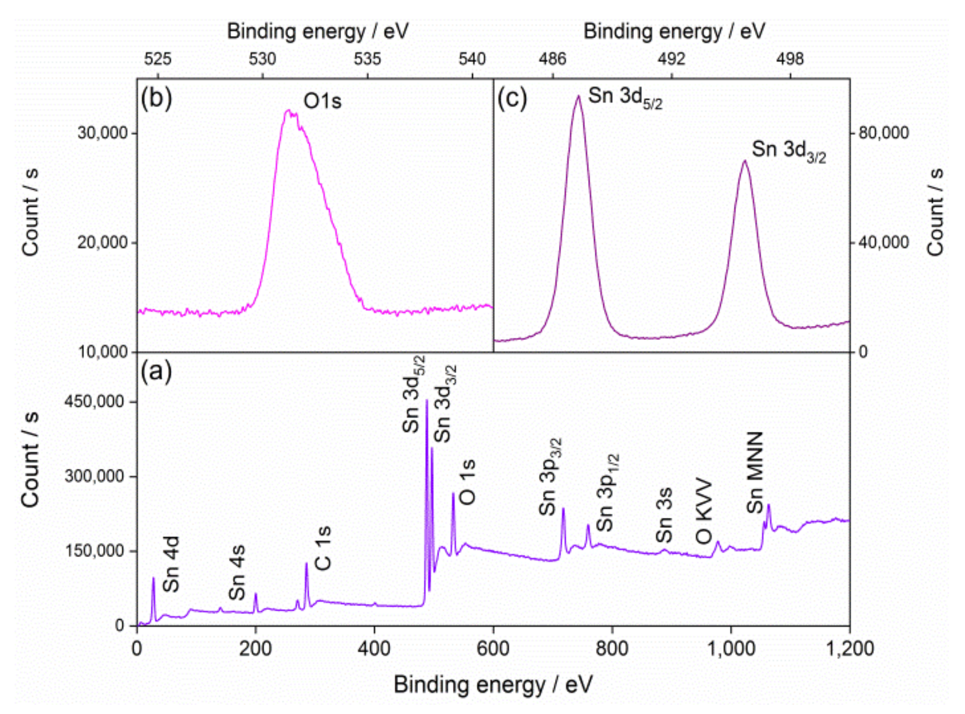
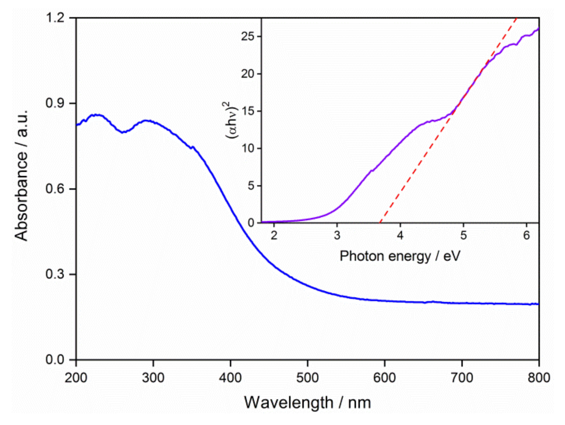
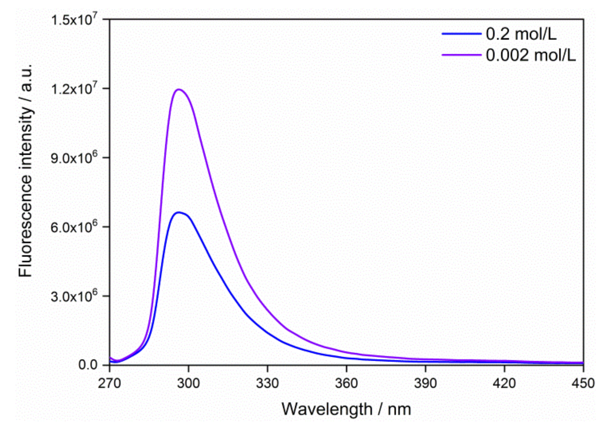
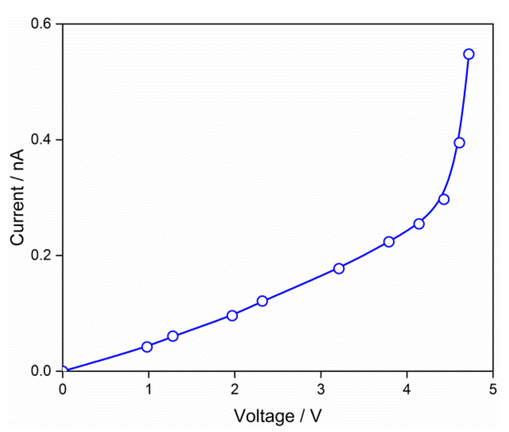
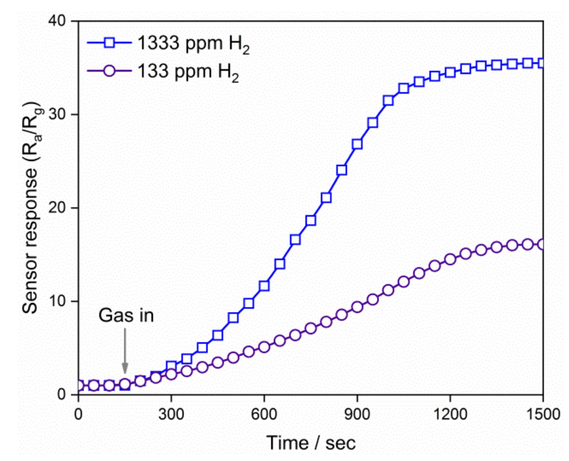
SnCl2·2H2O of 0.01 mol and CH4N2S of 0.001 mol were dissolved into deionized water of 50 ml by a magnet stirring apparatus in order to acquire a solution, which was stirred for 24 h at 25 °C. The starting material of SnCl2·2H2O was transformed to SnO2 QDs after hydrolysis and oxidation, which were promoted by the existence of CH4N2S, as shown in Equation (1) and Equation (2). It was proved that this process was spontaneous but the resultant was not stable [28,29]. CH4N2S acted as stabilizer and accelerator because of the tautomerism between thiourea and isothiourea in the acidic solution [30,31]. It therefore consumed the HCl and accelerated the ongoing of Equation (1) as well as the formation of SnO2 QDs.
SnCl2 + 2H2O→Sn(OH)2 + 2HCl
2Sn(OH)2 + O2→2SnO2 + 2H2O
The obtained SnO2 QD solution was tagged as QD0, and it was put into the polyphenylene autoclave for hydrothermal treatment at 125 and 225 °C for 2 h, with QD125 and QD225 tags for the corresponding samples, respectively. The QD solutions were dried to obtain powders for compositional and optical characterizations. The QD0 solution was deposited on alumina substrates with silver electrodes, which were described in previous work [12]. The deposition process of QD thin film comprised a spin-coating at 1000 rpm and a subsequent heat treatment at 150 °C for 10 min. The deposition was repeated five times, and the obtained thin film was used for characterization of electrical and gas-sensing properties.
The morphology of SnO2 QDs were observed by transmission electron microscopy (TEM, JEM-3200FS, JEOL, Tokyo, Japan). The QD size distribution was obtained by dynamic light scattering (DLS, Zetasizer Nano ZS 90, Malvern panalytical Ltd., Malvern, UK). The dried powders were prepared for X-ray diffraction analysis (XRD, D/MAX-Ultima, Rigaku, Tokyo, Japan), X-ray photoelectron spectroscopy (XPS, ESCALAB 250 XI, ThermoFisher Scientific, Waltham, MA, USA), and ultraviolet–visible spectroscopy (UV-VIS, UH4150 Spectrophotometer, Hitachi, Tokyo, Japan). The fluorescence spectra of the QD0 solution and its diluted one were collected by a fluorescence spectrometer (FLS-980, Edinburgh Instruments, Edinburgh, UK). The electrical property and gas-sensing characteristics of QD0 thin films were measured by Keithley 2450 (Tektronix, Beaverton, OR, USA). The sensor response (S) was defined as the ratio of the thin film resistance in air (Ra) to the ratio in the reducing gas (Rg), as S = Ra/Rg. H2 was used as the representative of reducing target gases in order to check the gas-sensing characteristics of SnO2 QDs.

3. Results

Figure 1 illustrates the morphologies of SnO2 QDs from TEM observation, which shows the average grain sizes of 1.9 ± 0.2, 2.7 ± 0.4, and 3.9 ± 0.8 nm for QD0, QD125, and QD225 samples, respectively. The grains appeared to be uniform in size. QD0 and QD125 samples dispersed well in the aqueous solution, while a little aggregation was found in the QD225 sample. The characteristic spacing of 0.33 nm was observed, corresponding to the (110) planes of the rutile phase of SnO2.
The XRD patterns of QD0, QD125, and QD225 samples are revealed in Figure 2, in which the standard pattern of SnO2 peaks [32] was also involved. An extremely weak peak was observed for the (211) plane of the QD0 sample. After the hydrothermal treatment at 125 °C, the grain growth happened as the obvious (211) peak appeared. The whole SnO2 peak pattern was found when the temperature of hydrothermal treatment increased to 225 °C, as shown by the QD225 sample, which showed a complete crystal structure of the rutile SnO2 system. The crystallite size of each sample was calculated by the Scherrer’s formula based on the (211) peak. The QD125 and QD225 samples had crystallite sizes of 2.8 nm and 4.2 nm, respectively, while the crystallite size was less than 2.0 nm in the QD0 sample. The results were in agreement with the TEM observation.
Figure 3 shows the size distributions of QD0, QD125, and QD225 samples in aqueous solution. The peaks appeared at 4.8, 5.6, and 6.5 nm, shifting to larger sizes with the incremental temperature of the hydrothermal process. The average grain sizes were 5.3 ± 1.1, 5.8 ± 0.9, and 8.0 ± 5.9 nm, respectively, and the results were larger than the ones from TEM observation and the XRD calculation. The results of TEM, XRD, and DLS showed that hydrothermal treatment is an effective way to control the grain size of SnO2 QDs. The grains grew up in the aqueous solution by combining tiny crystallites of SnO2, and the higher temperature of hydrothermal treatment provided more energy for combination. Therefore, it was possible to prepare desired QDs with controllable grain sizes by adjusting the temperature and time of hydrothermal treatment.
Figure 4a shows the survey XPS spectrum of the QD0 sample, which performed the existence of C, O, and Sn elements. Two peaks of 487.3 and 495.6 eV were observed in the high solution pattern of Sn 3d, corresponding to Sn 3d3/2 and Sn 3d5/2, as shown in Figure 4c. Meanwhile, the peak of O 1s appeared at 531.5 eV, as shown in Figure 4b. The results coincided with the standard pattern from the rutile SnO2 system [33,34].
The UV-VIS absorption spectrum of the QD0 sample is shown in Figure 5, which shows two absorption peaks. The spectrum was transformed and plotted in the coordinates of (αhν)2 against in order to evaluate the band gap (Eg). The Eg was calculated to be 3.66 eV, with a slight increase compared to 3.6 eV of the bulk SnO2 material. The Eg increase of SnO2 QDs was also concluded in other works [13,25,35]. However, the evaluated Eg was smaller than the ones in the previous reports for QDs with similar sizes. The defects in the crystal lattice, such as oxygen vacancies, were potentially responsible for the slight enhancement of Eg.
The fluorescence spectra of the QD0 sample with the concentration of 0.2 and 0.002 mol/L are shown in Figure 6. The emission peaks at 300 nm were in agreement with the previous report [36]. The fluorescence quenching was observed when the concentration was as high as 0.2 mol/L. In this case, the fluorescence emission was inhibited by the nearby grains, which adsorbed the energy of electron transition from conduction band to valence band. It was ascribed to the self-quenching of fluorescence, which is the strong coupling of ground state fluorescence agents creating a stable, non-fluorescent complex [37]. The fluorescence self-quenching was driven by hydrophobic effects or π-π stacking of fluorescence agents at high concentrations [38].
Figure 7 shows the voltage-current characteristics of the thin film, which was prepared from the QD0 solution. An approximately linear curve was observed between 0 and 4 V. A sharp increase took place when the voltage increased to 4–5 V. In this case, the depletion layer disappeared under the effect of an external biased electric field. The tendency of the curve was similar to the nanocrystalline SnO2 thin films with Schottky barrier at grain boundaries [39], revealing that the electrical properties of the QD thin film were also determined by the depletion layer.
Figure 8 shows the dynamic response of the QD0 thin film at room temperature to the H2 gas with concentration of 133 and 1333 ppm, to which the responses are 16.1 and 35.5. After exposure to the reducing gas, the resistance of thin film decreased, because the reducing gas molecules consumed the adsorbed oxygen on the grain surface. The results show that the SnO2 gas sensor benefited from the structure of the QDs. Van Toan [40] used to fabricate SnO2 nanocrystalline gas sensors with grain size of 20 nm, which showed a response of 6 to 1000 ppm H2 at 300 °C. Kim [41] recently prepared SnO2 nanowire-based gas sensors, and the response of bare SnO2 nanowires was 8 to 100 ppm H2 at 300 °C. Therefore, the prepared QDs were the promising candidate for producing novel semiconductor gas sensors, which were highly sensitive at room temperature. In this work, however, only the gas of H2 was used to check the gas-sensing performance of QDs, as was the same operation in much other research [42,43]. It is known that the semiconductor gas sensors would show response to other gases, such as CO, NO2, ammonia, and acetone [44]. Thus, selectivity was one of the sensor properties that had to be concerned. The sensor properties were also found to be dependent on the characteristics of QDs, including grain size and shape [45,46,47,48]. Further investigations are expected to reveal the details of gas-sensing performances, including the grain size effect and selectivity of the semiconductor QDs.

4. Conclusions

The SnO2 QDs were prepared in the aqueous solution via a simple process of hydrolysis and oxidation. The average grain size was 1.9 nm, and it increased to 2.7 and 4.0 nm after the hydrothermal treatments at 125 and 225 °C, respectively. The rutile SnO2 system was confirmed by the XPS spectrum and the XRD pattern. UV-VIS absorption spectrum results had an Eg value of 3.66 eV, which is a little larger than the bulk SnO2 system. The QDs of 0.002 mol/L showed a fluorescence emission peak at the wavelength of 300 nm, and their fluorescence response was quenched when the high concentration of 0.2 mol/L was used. The voltage-current characteristics showed that the electrical properties of the QD thin film were determined by the depletion layer, where a Schottky barrier was established at the grain boundaries. The QD thin film showed responses of 16.1 and 35.5 to H2 gas with concentration of 133 and 1333 ppm, respectively.

Author Contributions

Methodology, J.Lv.; investigation, J.Lv., W.X., J.Lv., and W.H.; writing—original draft preparation, J.Lv. & W.X.; writing—review and editing, Z.Z. & G.J.; supervision, Y.C.; project administration, J.Lv. & G.J.; funding acquisition, J.Lv.

Funding

This work was financially supported by the National Natural Science Foundation of China (Grant No. 11704055), the Liaoning Natural Science Foundation (Grant No. 20180510021), the Dalian High-Level Talents Innovation Supporting Program (Grant No. 2017RQ073), and the Fundamental Research Funds for the Central Universities (Grant No. 3132018188, 3132016320, and 3132016347).

Conflicts of Interest

The authors declare no conflicts of interest.

References

  1. Maulu, A.; Navarro-Arenas, J.; Rodríguez-Cantó, P.J.; Sánchez-Royo, J.F.; Abargues, R.; Suárez, I.; Martínez-Pastor, J.P. Charge transport in trap-sensitized infrared PbS quantum-dot-based photoconductors: Pros and cons. Nanomaterials 2018, 8, 677. [Google Scholar] [CrossRef] [PubMed]
  2. Yuan, C.; Li, L.; Huang, J.; Ning, Z.; Sun, L.; Ågren, H. Improving the photocurrent in quantum-dot-sensitized solar cells by employing alloy PbxCd1−xS quantum dots as photosensitizers. Nanomaterials 2016, 6, 97. [Google Scholar] [CrossRef] [PubMed]
  3. Mohamed, A.E.; Yuangang, Z.; Hsiao-Hua, Y.; Ying, J.Y. Ultrasensitive Pb2+ detection by glutathione-capped quantum dots. Anal. Chem. 2007, 79, 9452–9458. [Google Scholar] [CrossRef] [PubMed]
  4. Silva do Nascimento, A.; Cabral Filho, P.E.; Fontes, A.; Saegesser Santos, B.; Rodrigues de Carvalho, F.; Stragevitch, L.; Soares Leite, E. CdSe quantum dots as fluorescent nanomarkers for diesel oil. Fuel 2019, 239, 1055–1060. [Google Scholar] [CrossRef]
  5. Zhang, B.; Li, M.; Song, Z.; Kan, H.; Yu, H.; Liu, Q.; Zhang, G.; Liu, H. Sensitive H2S gas sensors employing colloidal zinc oxide quantum dots. Sens. Actuators B 2017, 249, 558–563. [Google Scholar] [CrossRef]
  6. Liu, H.; Li, M.; Shao, G.; Zhang, W.; Wang, W.; Song, H.; Cao, H.; Ma, W.; Tang, J. Enhancement of hydrogen sulfide gas sensing of PbS colloidal quantum dots by remote doping through ligand exchange. Sens. Actuators B 2015, 212, 434–439. [Google Scholar] [CrossRef]
  7. Li, M.; Luo, J.; Fu, C.; Kan, H.; Huang, Z.; Huang, W.; Yang, S.; Zhang, J.; Tang, J.; Fu, Y.; et al. PbSe quantum dots-based chemiresistors for room-temperature NO2 detection. Sens Actuators B 2018, 256, 1045–1056. [Google Scholar] [CrossRef]
  8. Liu, H.; Li, M.; Voznyy, O.; Hu, L.; Fu, Q.; Zhou, D.; Xia, Z.; Sargent, E.H.; Tang, J. Physically flexible, rapid-response gas sensor based on colloidal quantum dot solids. Adv. Mater. 2014, 26, 2718–2724. [Google Scholar] [CrossRef]
  9. Song, Z.; Huang, Z.; Liu, J.; Hu, Z.; Zhang, J.; Zhang, G.; Yi, F.; Jiang, S.; Lian, J.; Yan, J. Fully stretchable and humidity-resistant quantum dot gas sensors. ACS Sens. 2018, 3, 1048–1055. [Google Scholar] [CrossRef]
  10. Zepeda, A.M.; Gonzalez, D.; Heredia, L.G.; Marquez, K.; Perez, C.; Pena, E.; Flores, K.; Valdes, C.; Eubanks, T.M.; Parsons, J.G. Removal of Cu2+ and Ni2+ from aqueous solution using SnO2 nanomaterial effect of: pH, time, temperature, interfering cations. Microchem. J. 2018, 141, 188–196. [Google Scholar] [CrossRef]
  11. Liu, J.; Lu, Y.; Cui, X.; Geng, Y.; Jin, G.; Zhai, Z. Gas-sensing properties and sensitivity promoting mechanism of Cu-added SnO2 thin films deposited by ultrasonic spray pyrolysis. Sens. Actuators B 2017, 248, 862–867. [Google Scholar] [CrossRef]
  12. Liu, J.; Liu, X.; Zhai, Z.; Jin, G.; Jiang, Q.; Zhao, Y.; Luo, C.; Quan, L. Evaluation of depletion layer width and gas-sensing properties of antimony-doped tin oxide thin film sensors. Sens. Actuators B 2015, 220, 1354–1360. [Google Scholar] [CrossRef]
  13. Song, Z.; Liu, J.; Liu, Q.; Yu, H.; Zhang, W.; Wang, Y.; Huang, Z.; Zang, J.; Liu, H. Enhanced H2S gas sensing properties based on SnO2 quantum wire/reduced graphene oxide nanocomposites: Equilibrium and kinetics modeling. Sens. Actuators B 2017, 249, 632–638. [Google Scholar] [CrossRef]
  14. Liu, H.; Zhang, W.; Yu, H.; Liang, G.; Song, Z.; Xu, S.; Min, L.; Yang, W.; Song, H.; Jiang, T. Solution-processed gas sensors employing SnO2 quantum dot/MWCNT Nanocomposites. ACS Appl. Mater. Interfaces 2016, 8, 840. [Google Scholar] [CrossRef] [PubMed]
  15. Liu, J.; Wang, W.; Zhai, Z.; Jin, G.; Chen, Y.; Hong, W.; Wu, L.; Gao, F. Influence of oxygen vacancy behaviors in cooling process on semiconductor gas sensors: A numerical analysis. Sensors 2018, 18, 3929. [Google Scholar] [CrossRef] [PubMed]
  16. Liu, J.; Wang, W.; Zhai, Z.; Jin, G.; Chen, Y. Numerical analysis of the effect of the cooling process on the characteristics of n-type semiconductor gas sensors. J. Comput. Electron. 2018. [Google Scholar] [CrossRef]
  17. Liu, J.; Gao, Y.; Wu, X.; Jin, G.; Zhai, Z.; Liu, H. Inhomogeneous oxygen vacancy distribution in semiconductor gas sensors: Formation, migration and determination on gas sensing characteristics. Sensors 2017, 17, 1852. [Google Scholar] [CrossRef]
  18. Zhao, D.; Wu, X. Nanoparticles assembled SnO2 nanosheet photocatalysts for wastewater purification. Mater. Lett. 2018, 210, 354–357. [Google Scholar] [CrossRef]
  19. Tammina, S.K.; Mandal, B.K.; Khan, F.N. Mineralization of toxic industrial dyes by gallic acid mediated synthesized photocatalyst SnO2 nanoparticles. Environ. Technol. Innov. 2019, 13, 197–210. [Google Scholar] [CrossRef]
  20. Jayaweera, E.N.; Kumara, G.R.A.; Kumarage, C.; Ranasinghe, S.K.; Rajapakse, R.M.G.; Bandara, H.M.N.; Ileperuma, O.A.; Dassanayake, B.S. CdS nanosheet-sensitized solar cells based on SnO2/MgO composite films. J. Photochem. Photobiol. A 2018, 364, 109–115. [Google Scholar] [CrossRef]
  21. Zhang, X.; Rui, Y.; Yang, J.; Wang, L.; Wang, Y.; Xu, J. Monodispersed SnO2 microspheres aggregated by tunable building units as effective photoelectrodes in solar cells. Appl. Surf. Sci. 2019, 463, 679–685. [Google Scholar] [CrossRef]
  22. Min, X.; Sun, B.; Chen, S.; Fang, M.; Wu, X.; Liu, Y.G.; Abdelkader, A.; Huang, Z.; Liu, T.; Xi, K.; et al. A textile-based SnO2 ultra-flexible electrode for lithium-ion batteries. Energy Storage Mater. 2019, 16, 597–606. [Google Scholar] [CrossRef]
  23. Li, H.; Su, Q.; Kang, J.; Huang, M.; Feng, M.; Feng, H.; Huang, P.; Du, G. Porous SnO2 hollow microspheres as anodes for high-performance lithium ion battery. Mater. Lett. 2018, 217, 276–280. [Google Scholar] [CrossRef]
  24. Hollingsworth, J.A. Semiconductor Nanocrystal Quantum Dots; John Wiley & Sons, Ltd.: Hoboken, NJ, USA, 2006. [Google Scholar]
  25. Song, Z.; Xu, S.; Liu, J.; Hu, Z.; Gao, N.; Zhang, J.; Yi, F.; Zhang, G.; Jiang, S.; Liu, H. Enhanced catalytic activity of SnO2 quantum dot films employing atomic ligand-exchange strategy for fast response H2S gas sensors. Sens. Actuators B 2018, 271, 147–156. [Google Scholar] [CrossRef]
  26. Liu, H.; Xu, S.; Min, L.; Gang, S.; Song, H.; Zhang, W.; Wei, W.; He, M.; Liang, G.; Song, H. Chemiresistive gas sensors employing solution-processed metal oxide quantum dot films. Appl. Phys. Lett. 2014, 105, 766. [Google Scholar] [CrossRef]
  27. Babu, B.; Neelakanta Reddy, I.; Yoo, K.; Kim, D.; Shim, J. Bandgap tuning and XPS study of SnO2 quantum dots. Mater. Lett. 2018, 221, 211–215. [Google Scholar] [CrossRef]
  28. Han, W.-Q.; Zettl, A. Coating single-walled carbon nanotubes with tin oxide. Nano Lett. 2003, 3, 681–683. [Google Scholar] [CrossRef]
  29. Cigala, R.M.; Crea, F.; de Stefano, C.; Lando, G.; Milea, D.; Sammartano, S. The inorganic speciation of tin(II) in aqueous solution. Geochim. Cosmochim. Acta 2012, 87, 1–20. [Google Scholar] [CrossRef]
  30. Misra, G.S.; Gupta, C.V. Aqueous polymerization of methacrylamide initiated by acidified bromate/thiourea redox system. Die Makromol. Chem. 1973, 168, 105–118. [Google Scholar] [CrossRef]
  31. Swaminathan, K.; Irving, H.M.N.H. Infra-red absorption spectra of complexes of thiourea. J. Inorg. Nucl. Chem. 1964, 26, 1291–1294. [Google Scholar] [CrossRef]
  32. Seki, H.; Ishisawa, N.; Mizutani, N.; Kato, M. High temperature structures of the rutile-type oxides, TiO2 and SnO2. J. Ceram. Assoc. Jpn. 1984, 92, 219–223. [Google Scholar] [CrossRef]
  33. Barreca, D.; Garon, S.; Tondello, E.; Zanella, P. SnO2 nanocrystalline thin films by XPS. Surf. Sci. Spectra 2000, 7, 81–85. [Google Scholar] [CrossRef]
  34. Stranick, M.A.; Moskwa, A. SnO2 by XPS. Surf. Sci. Spectra 1993, 2, 50–54. [Google Scholar] [CrossRef]
  35. Song, Z.; Wei, Z.; Wang, B.; Zhen, L.; Xu, S.; Zhang, W.; Yu, H.; Min, L.; Zhao, H.; Zang, J. Sensitive room-temperature H2S gas sensors employing SnO2 quantum wire/reduced graphene oxide nanocomposites. Chem. Mater. 2016, 28, 1205–1212. [Google Scholar] [CrossRef]
  36. Henry, J.; Mohanraj, K.; Sivakumar, G.; Umamaheswari, S. Electrochemical and fluorescence properties of SnO2 thin films and its antibacterial activity. Spectrochim. Acta Part A 2015, 143, 172–178. [Google Scholar] [CrossRef] [PubMed]
  37. Lakowicz, J.R. Quenching of Fluorescence. In Principles of Fluorescence Spectroscopy; Springer: New York, NY, USA, 2006; pp. 278–327. [Google Scholar]
  38. Zhai, D.; Xu, W.; Zhang, L.; Chang, Y.-T. The role of “disaggregation” in optical probe development. Chem. Soc. Rev. 2014, 43, 2402–2411. [Google Scholar] [CrossRef] [PubMed]
  39. Gong, S.; Liu, J.; Quan, L.; Fu, Q.; Zhou, D. Preparation of tin oxide thin films on silicon substrates via sol-gel routes and the prospects for the H2S gas sensor. Sens. Lett. 2011, 9, 625–628. [Google Scholar] [CrossRef]
  40. Van Toan, N.; Viet Chien, N.; Van Duy, N.; Si Hong, H.; Nguyen, H.; Duc Hoa, N.; Van Hieu, N. Fabrication of highly sensitive and selective H2 gas sensor based on SnO2 thin film sensitized with microsized Pd islands. J. Hazard. Mater. 2016, 301, 433–442. [Google Scholar] [CrossRef]
  41. Kim, J.-H.; Mirzaei, A.; Kim, H.W.; Kim, S.S. Improving the hydrogen sensing properties of SnO2 nanowire-based conductometric sensors by Pd-decoration. Sens. Actuators B 2019, 285, 358–367. [Google Scholar] [CrossRef]
  42. Sakai, G.; Matsunaga, N.; Shimanoe, K.; Yamazoe, N. Theory of gas-diffusion controlled sensitivity for thin film semiconductor gas sensor. Sens. Actuators B 2001, 80, 125–131. [Google Scholar] [CrossRef]
  43. Xu, C.; Tamaki, J.; Miura, N.; Yamazoe, N. Grain size effects on gas sensitivity of porous SnO2-based elements. Sens. Actuators B 1991, 3, 147–155. [Google Scholar] [CrossRef]
  44. Krivetskiy, V.; Ponzoni, A.; Comini, E.; Badalyan, S.; Rumyantseva, M.; Gaskov, A. Selectivity modification of SnO2-based materials for gas sensor arrays. Electroanalysis 2010, 22, 2809–2816. [Google Scholar] [CrossRef]
  45. Yamazoe, N.; Shimanoe, K. Roles of shape and size of component crystals in semiconductor gas sensors II. Response to NO2 and H2. J. Electrochem. Soc. 2008, 155, J93–J98. [Google Scholar] [CrossRef]
  46. Yamazoe, N.; Shimanoe, K. Roles of shape and size of component crystals in semiconductor gas sensors I. Response to oxygen. J. Electrochem. Soc. 2008, 155, J85–J92. [Google Scholar] [CrossRef]
  47. Liu, J.; Zhai, Z.; Jin, G.; Li, Y.; Monica, F.F.; Liu, X. Simulation of the grain size effect in gas-sensitive SnO2 thin films using the oxygen vacancy gradient distribution model. Electron. Mater. Lett. 2015, 11, 34–40. [Google Scholar] [CrossRef]
  48. Liu, J.; Jin, G.; Zhai, Z.; Monica, F.F.; Liu, X. Numeral description of grain size effects of tin oxide gas-sensitive elements and evaluation of depletion layer width. Electron. Mater. Lett. 2015, 11, 457–465. [Google Scholar] [CrossRef]
Figure 1. Transmission electron microscope morphologies of quantum dot (QD) samples: (a) QD0, (b) QD125, and (c) QD225.
Nanomaterials 09 00240 g001
Figure 2. X-ray diffraction patterns of QD0, QD125, and QD225 samples with the standard pattern of SnO2 semiconductors.
Nanomaterials 09 00240 g002
Figure 3. Size distributions of QD0, QD125, and QD225 samples in aqueous solution.
Nanomaterials 09 00240 g003
Figure 4. X-ray photoelectron spectrum of the QD0 sample: (a) Survey and high-solution peaks of (b) O 1s and (c) Sn 3d.
Nanomaterials 09 00240 g004
Figure 5. Ultraviolet-visible absorption spectrum of the QD0 sample and the evaluation of band gap (Eg).
Nanomaterials 09 00240 g005
Figure 6. Fluorescence spectra of the QD0 sample with concentration of 0.2 and 0.002 mol/L.
Nanomaterials 09 00240 g006
Figure 7. Voltage-current characteristics of the thin film prepared from the QD0 solution.
Nanomaterials 09 00240 g007
Figure 8. Gas-sensing characteristics of the thin film prepared from the QD0 solution at room temperature.
Nanomaterials 09 00240 g008

